Analysis apparatus and electronic device

an analysis apparatus and electronic device technology, applied in the direction of instruments, optical radiation measurement, spectroscopy, etc., can solve the problems of insufficient and low enhancement degree, and achieve the effect of high sensitivity, high sensitivity and enhanced degr

Inactive Publication Date: 2015-08-20
SEIKO EPSON CORP
View PDF17 Cites 6 Cited by
  • Summary
  • Abstract
  • Description
  • Claims
  • Application Information

AI Technical Summary

Benefits of technology

[0010]An advantage of some aspects of the invention is to provide an analysis apparatus and an electronic device in which a high enhancement degree is obtained in an enhancement degree spectrum, and a target substance is able to be detected and analyzed with high sensitivity. Another advantage of some aspects of the invention is to provide an analysis apparatus and an electronic device in which the target substance is easily attached to a position having a high enhancement degree. Still another advantage of some aspects of the invention is to provide an analysis apparatus and an electronic device in which an allowable range of a variation in manufacturing is wide.
[0013]According to the analysis apparatus, an extremely high enhancement degree is obtained in an enhancement degree spectrum, and a target substance is able to be detected and analyzed with high sensitivity. In addition, a position in which a high enhancement degree of the analysis apparatus is obtained exists on at least an upper surface side of metallic particles, and thus the target substance is easily in contact with the position, and it is possible to detect and analyze the target substance with high sensitivity. Further, this analysis apparatus satisfies a relationship of 40 [nm]≦G·(neff / 1.46), and thus it is possible to increase an allowable range of a variation in manufacturing.
[0015]According to the analysis apparatus, an extremely high enhancement degree is obtained in an enhancement degree spectrum, and a target substance is able to be detected and analyzed with high sensitivity. In addition, a position in which a high enhancement degree of the analysis apparatus is obtained exists on at least an upper surface side of metallic particles, and thus the target substance is easily in contact with the position, and it is possible to detect and analyze the target substance with high sensitivity. Further, this analysis apparatus satisfies a relationship:40[nm]≦∑m=1m{(Gm·cosθm)·(nm / 1.46)}and thus it is possible to increase an allowable range of a variation in manufacturing.
[0017]According to the analysis apparatus with this configuration, an extremely high enhancement degree is obtained in an enhancement degree spectrum, and a target substance is able to be detected and analyzed with high sensitivity.
[0025]In this case, according to the analysis apparatus, even when the thickness of the light-transmissive layer varies, the ratio of the intensity of the localized surface plasmon excited to an upper surface side of the metallic particles to the intensity of the localized surface plasmon excited to a lower surface side of the metallic particles does not vary, and thus the analysis apparatus is more easily manufactured.
[0027]According to the electronic device, an enhancement degree is extremely high, and a target substance is able to be detected and analyzed with high sensitivity, and thus medical health information with high sensitivity and high accuracy is able to be provided.

Problems solved by technology

However, in a sensor having a structure disclosed in JP-T-2007-538264, it is found that a peak of an electric field enhancement degree in wavelength dependent properties (an enhancement degree spectrum or a reflectance spectrum) is broad, but an enhancement degree which is totally low and insufficient is obtained.

Method used


Image

  • Analysis apparatus and electronic device
  • Analysis apparatus and electronic device
  • Analysis apparatus and electronic device

Examples


experimental example

4. EXPERIMENTAL EXAMPLE

[0153]Hereinafter, the invention will be further described by using experimental examples, but the invention is not limited to the following examples.

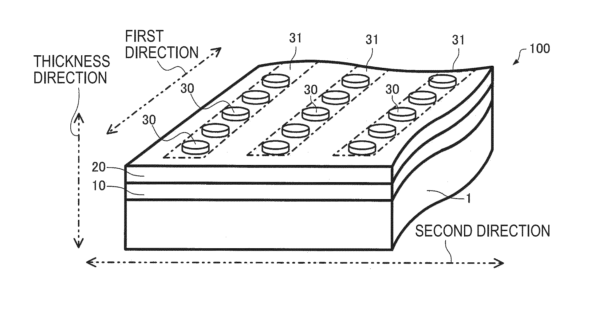
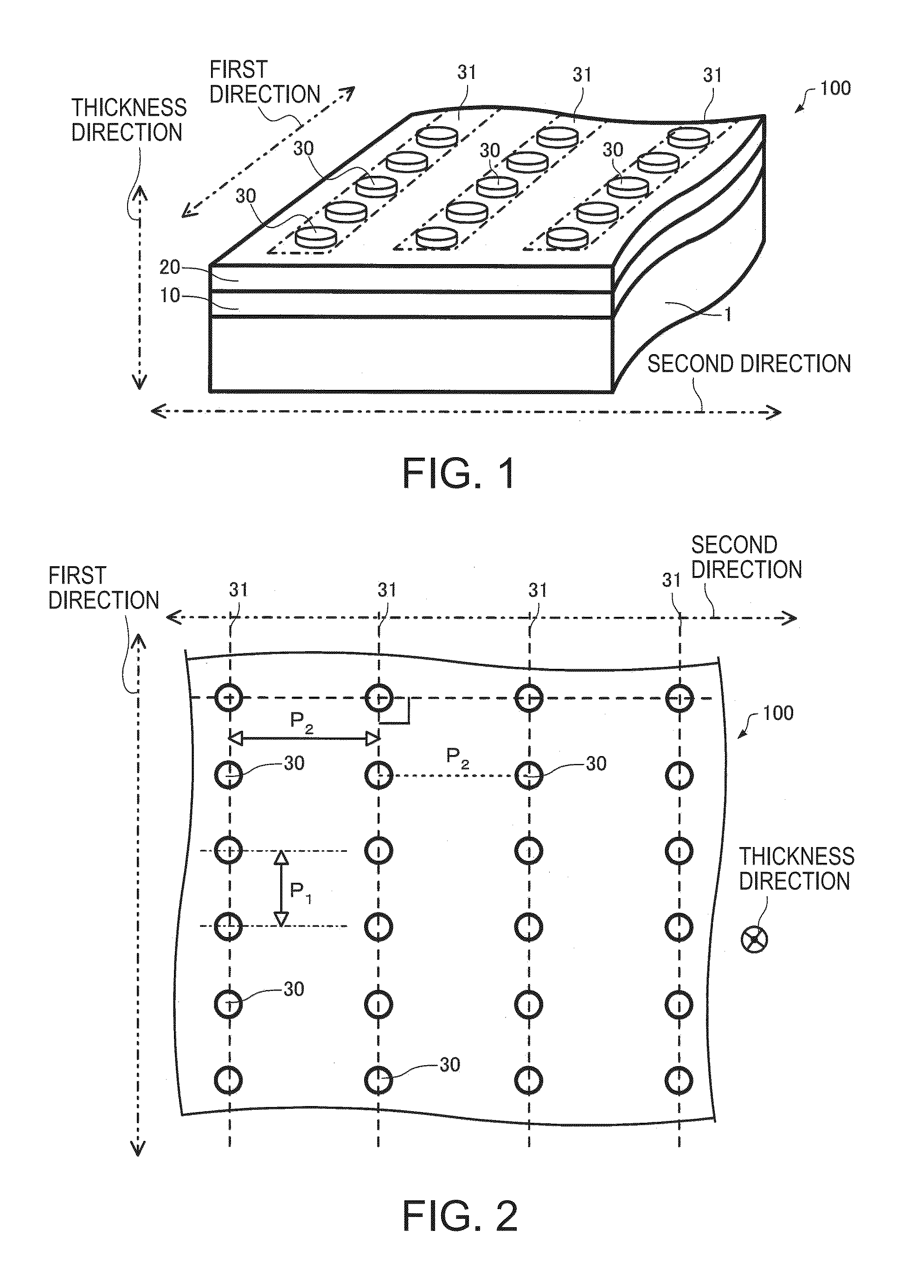
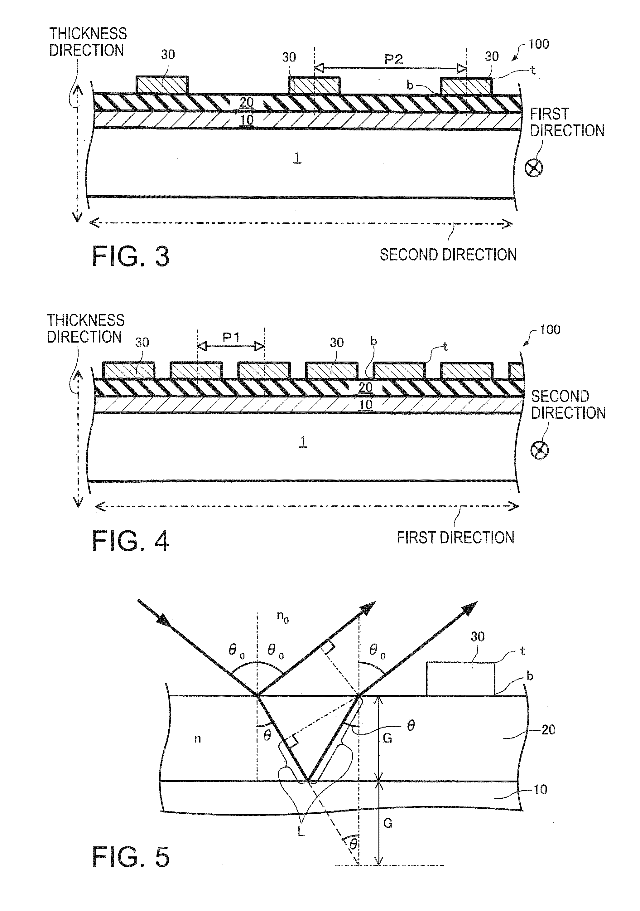
[0154]In each experimental example, the following model schematically illustrated in FIG. 12 is used.

[0155]As a metallic layer which is sufficiently thick to the extent that light is not transmitted, a gold (Au) layer is used, as a light-transmissive layer, a SiO2 layer having a refractive index of 1.46 is formed on the metallic layer (gold), and as metallic particles, cylindrical silver is formed on the light transmissive layer at a constant cycle, and thus a Gap type Surface Plasmon Polariton (GSPP) model is formed. Furthermore, a material of the metallic layer and the metallic particles is not limited, insofar as metal in which a real part of a dielectric constant negatively increases, and an imaginary part is smaller than the real part in a wavelength region of the excitation light is used, plasmon is able to...


PUM

PropertyMeasurementUnit
thicknessaaaaaaaaaa
sizeaaaaaaaaaa
electric fieldaaaaaaaaaa

Abstract

An analysis apparatus includes an electric field enhancing element including a metallic layer, a light-transmissive layer, and a plurality of metallic particles arranged in a first direction and a second direction intersecting with the first direction; a light source irradiating the electric field enhancing element with at least one of linearly polarized light polarized in the first direction, linearly polarized light polarized in the second direction, and circularly polarized light; and a detector, in which localized surface plasmon and propagating surface plasmon are electromagnetically interacted, and when a thickness of the light-transmissive layer is G [nm], an effective reflective index of the light-transmissive layer is neff, and a wavelength of the excitation light is λi [nm], a relationship of the following expression (1) is satisfied.20 [nm]<G·(neff / 1.46)≦140 [nm]·(λi / 785 [nm])  (1)

Description

BACKGROUND[0001]1. Technical Field[0002]The present invention relates to an analysis apparatus and an electronic device.[0003]2. Related Art[0004]Recently, a demand for medical diagnosis, food inspection, or the like has increased greatly, and there has been a need to develop a compact and high-speed sensing technology. Various sensors commencing with an electrochemical method have been considered, and an interest with respect to a sensor using a surface plasmon resonance (SPR) has increased because integration is possible, the cost is reduced, and any measurement environment may be used. For example, a technology which detects a presence or absence of adsorption of a substance such as a presence or absence of adsorption of an antigen in an antigen-antibody reaction by using surface plasmon generated in a metallic thin film disposed on a total reflection prism surface has been known.[0005]In addition, a method is also considered in which Raman scattering of a substance attached to a...

Claims


Application Information

Patent Timeline
Patent Type & Authority Applications(United States)
IPC IPC(8): G01N21/65A61B5/00G06F19/00
CPCG01N21/658G06F19/3431A61B5/742A61B5/7278A61B5/0075G01N21/554G01N33/483
Inventor SUGIMOTO, MAMORUENARI, MEGUMI
Owner SEIKO EPSON CORP
Why Eureka
Try Eureka