
FIXED ARRAY ACFs WITH MULTI-TIER PARTIALLY EMBEDDED PARTICLE MORPHOLOGY AND THEIR MANUFACTURING PROCESSES

a technology of partially embedded particles and fixed arrays, which is applied in the direction of film/foil adhesives, printed circuit manufacturing, transportation and packaging, etc., can solve the problems of high undesirable for high resolution connections, breakage or shortening of electric circuit connections, and microcavities in this portion of the carrier web that are not well adapted to hold conductive particles, etc., to achieve better contact resistance, higher peeling force, and particle capture rate

Active Publication Date: 2015-08-27
POLAROID IP BV
View PDF3 Cites 14 Cited by
  • Summary
  • Abstract
  • Description
  • Claims
  • Application Information

AI Technical Summary

Benefits of technology

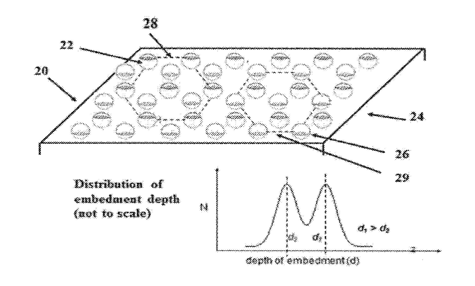
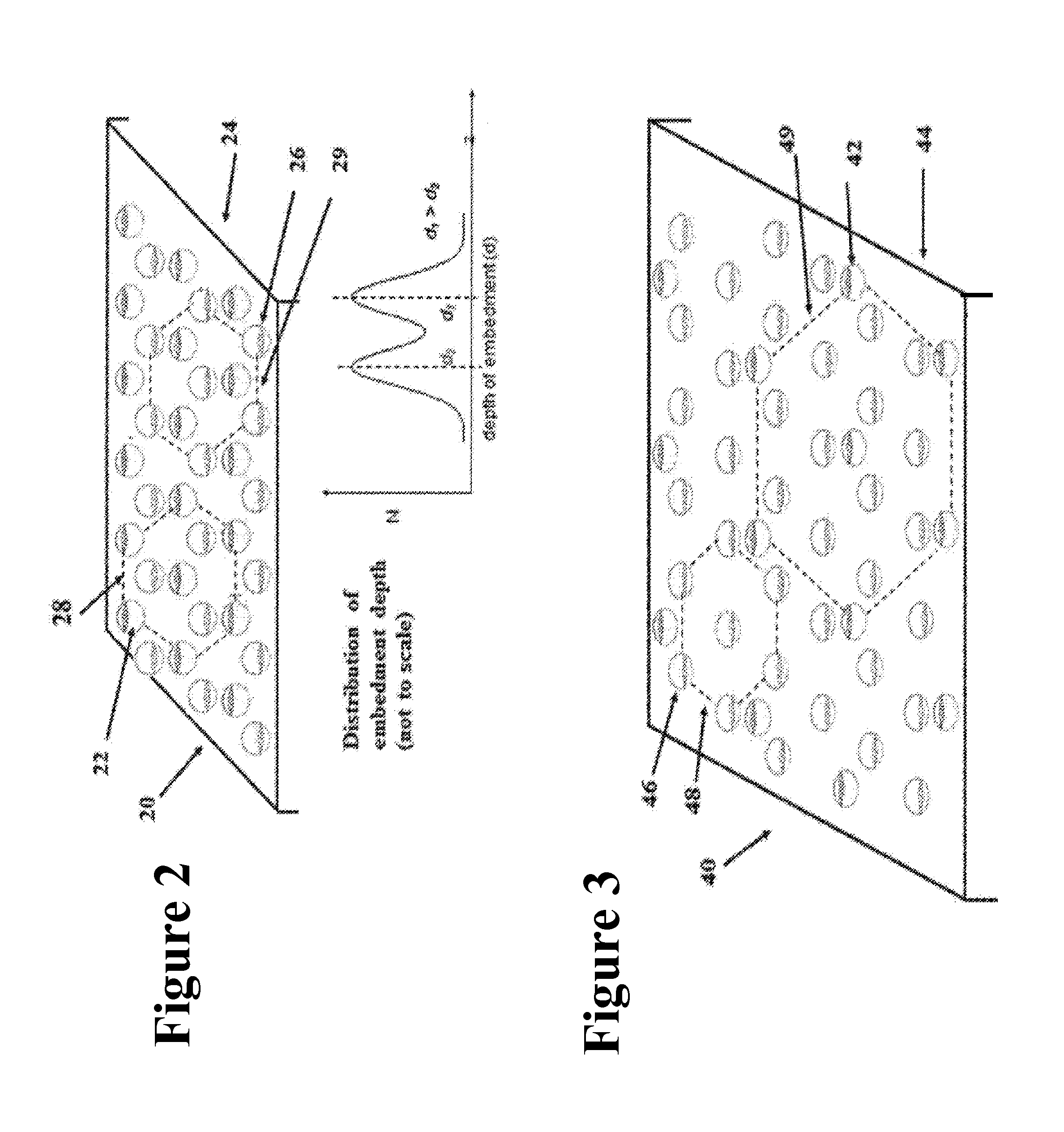
The patent text describes a new type of adhesive film (ACF) that is used in high-resolution integrated circuit (IC) bonding. The ACF has conductive particles embedded in its surface and a stitching line that is formed by the area where two parts of the ACF meet. The stitching line is important for bonding but can cause problems if it is not properly formed. The new ACF solves this issue by using a two-tier structure where conductive particles are embedded in the adhesive layer at different depths. This results in a higher particle capture rate, better contact resistance, and higher peeling force compared to a single-tier ACF. The stitching line is also overcoated with conductive particles to further improve bonding. The patent text also describes a method for manufacturing this new ACF.

Problems solved by technology

The microcavities in this portion of the carrier web are not well adapted to hold conductive particles.
An ACF with conductive particle aggregation will result in breaks or shorts in the electric circuit connections and is highly undesirable for any high resolution connections.
However, the tapered edge approach tends to result in a significantly wider stitching line and potential damage of the microcavity array along the tapered lines.
Both trade-offs will result in missing conductive particles and poor connectivity along the stitching line for high resolution applications.
Unfortunately, filling and curing the adhesive into the narrow trench of high aspect ratio is an extremely difficult and time-consuming process.
The surface smoothness and durability of the filled trench are often far from acceptable for the heavy duty microfluidic particle transfer process involved in the making of fixed array ACFs.

Method used


Image

  • FIXED ARRAY ACFs WITH MULTI-TIER PARTIALLY EMBEDDED PARTICLE MORPHOLOGY AND THEIR MANUFACTURING PROCESSES
  • FIXED ARRAY ACFs WITH MULTI-TIER PARTIALLY EMBEDDED PARTICLE MORPHOLOGY AND THEIR MANUFACTURING PROCESSES
  • FIXED ARRAY ACFs WITH MULTI-TIER PARTIALLY EMBEDDED PARTICLE MORPHOLOGY AND THEIR MANUFACTURING PROCESSES

Examples


Embodiment Construction

[0034]U.S. Published Application 2010 / 0101700 and U.S. application Ser. No. 13 / 111,300 filed May 19, 2011 to Liang et al. are also incorporated herein, in their entirety, by reference.

[0035]A carrier sheet or belt containing microcavities of about 6 μm (diameter) by about 4 μm (depth) by about 3 μm (partition) that is useful in transferring the conductive particles to the surface of the adhesive layer can be prepared by laser ablation on an approximately 2 to 5 mil heat-stabilized polyimide (PI) or polyester film such as PET to form the microcavity carrier. The microcavity array web is filled by coating with a conductive particle dispersion using for examples a smooth rod, doctor blade or slot die. More than one filling may be employed to assure no unfilled microcavities. See Liang '300 and Liang '700.

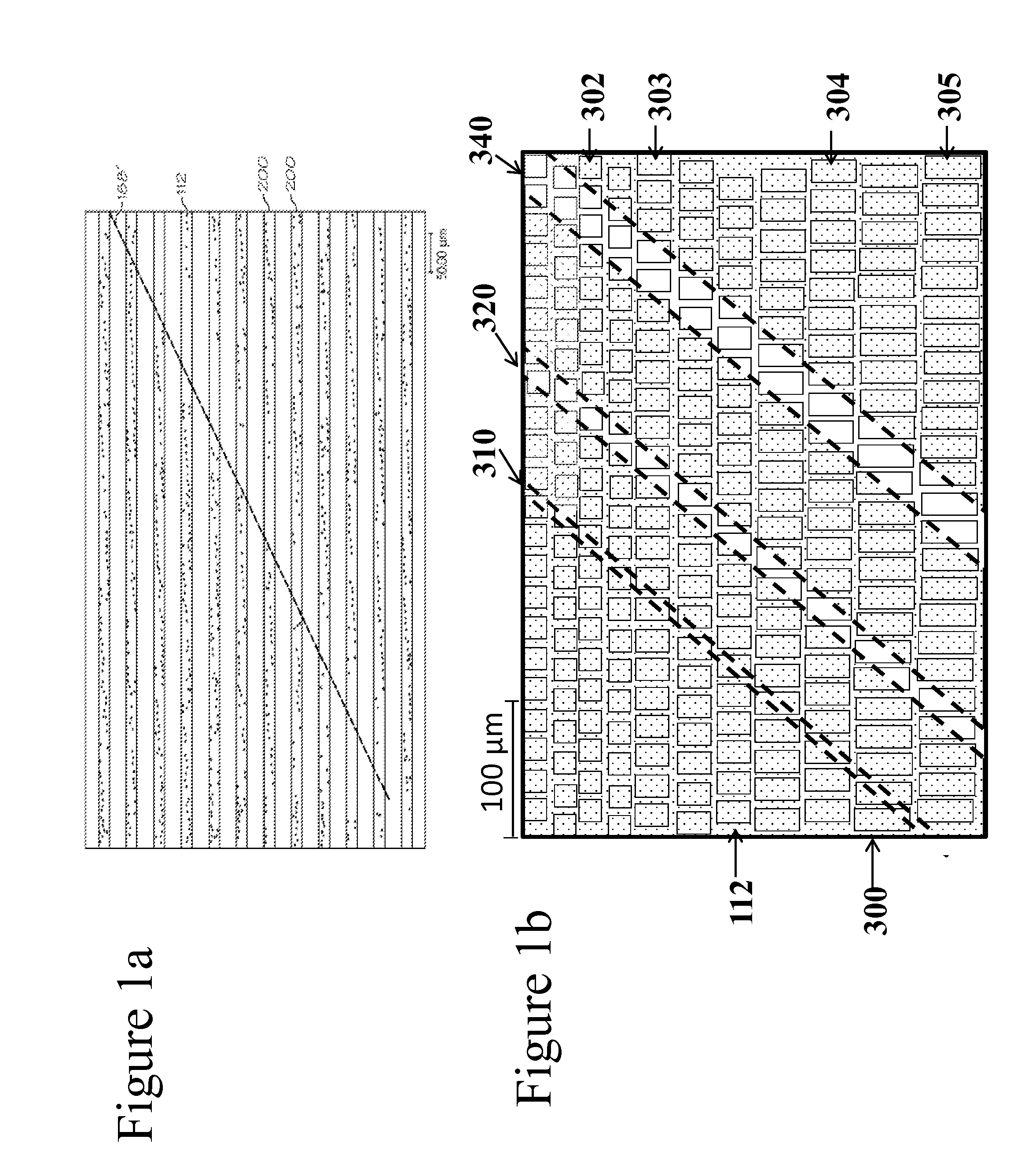
[0036]FIG. 1 is an illustration of a 400× photomicrograph of a bonded set of line electrodes of 18 μm (width)×1000 μm (length). The area 188′ corresponds to a 60° stitching line with a...


PUM

PropertyMeasurementUnit
Fractionaaaaaaaaaa
Fractionaaaaaaaaaa
Fractionaaaaaaaaaa

Abstract

An ACF comprising a substrate, a layer of an adhesive on the surface of the substrate, the adhesive optionally having conductive particles dispersed therein, at least one tier of conductive particles arranged in a non-random array, the tier being formed by transfer of conductive particles from a carrier belt having a stitching line to the surface of the adhesive layer wherein the portion of the tier corresponding to the stitching line is free of conductive particles, and the adhesive layer being overcoated with a second tier of conductive particles arranged in a non-random array at least in the area of the first tier corresponding to the stitching line. The tiers may be at the same or different depths within the adhesive layer. More than two tiers of conductive particles may be present in the ACF.

Description

CROSS-REFERENCE TO RELATED APPLICATIONS[0001]This application is a combined continuation-in-part of U.S. application Ser. No. 13 / 678,935 filed Nov. 16, 2012 (TS-023) and allowed U.S. application Ser. No. 13 / 233,360 filed Sep. 15, 2011 (TS-011). Both applications are incorporated herein by reference in their entireties.BACKGROUND[0002]Anisotropic Conductive Films (ACF) are commonly used in flat panel display driver integrated circuit (IC) bonding. A typical ACF bonding process comprises a first step in which the ACF is attached onto the electrodes of the panel glass; a second step in which the driver IC bonding pads are aligned with the panel electrodes; and a third step in which pressure and heat are applied to the bonding pads to melt and cure the ACF. The conductive particles of the ACF provide anisotropic electrical conductivity between the panel electrodes and the driver IC. ACF has also been used widely in applications such as flip chip bonding and photovoltaic module assembly....

Claims


Application Information

Patent Timeline
IPC IPC(8): C09J9/02C09J7/00C09J7/20
CPCC09J9/02C09J7/00C09J2203/326C09J2205/102C09J2201/602C08K7/04C08K7/16H05K3/323C08K2201/001C08K2201/005Y10T428/24C09J7/20Y10T428/24893C09J2301/314C09J2301/408
Inventor LIANG, RONG-CHANGSUN, JANECHU, HOWARD HO MANLEE, MENG-CHUN
Owner POLAROID IP BV
Learn More