Multi-layer thin-film coatings for system-in-package assemblies in portable electronic devices

a portable electronic device and multi-layer technology, applied in the direction of non-metallic protective coating application, electrical apparatus construction details, printed circuit non-printed electric components association, etc., can solve the problems of limiting the effectiveness of shielding, undesirable interference, and interference with the proper operation of another circuit, so as to reduce the size, enhance the form factor, and improve the effect of shielding

Active Publication Date: 2015-09-24
APPLE INC
View PDF5 Cites 9 Cited by
  • Summary
  • Abstract
  • Description
  • Claims
  • Application Information

AI Technical Summary

Benefits of technology

[0004]This relates to a compact portable electronic device and multi-layer thin-film coatings for System-in-Package assemblies. The compact portable electronic device can be assembled into a single package to reduce size and enhance form factor. Several tens or hundreds of electrical components including multiple dies, passive components, mechanical or optical co

Problems solved by technology

For example, some electronic devices include radio-frequency transceiver circuits that are susceptible to radio-frequency interference.
If care is not taken, signals from one circuit can interfere with the proper operation of another circuit.
For example, a clock signal or a clock signal harmonic that falls within the operating band of a radio-frequency receiver can cause undesirable interf

Method used


Image

  • Multi-layer thin-film coatings for system-in-package assemblies in portable electronic devices
  • Multi-layer thin-film coatings for system-in-package assemblies in portable electronic devices
  • Multi-layer thin-film coatings for system-in-package assemblies in portable electronic devices

Examples


Embodiment Construction

[0016]In the following description of examples, reference is made to the accompanying drawings in which it is shown by way of illustration specific examples that can be practiced. It is to be understood that other examples can be used and structural changes can be made without departing from the scope of the various examples.

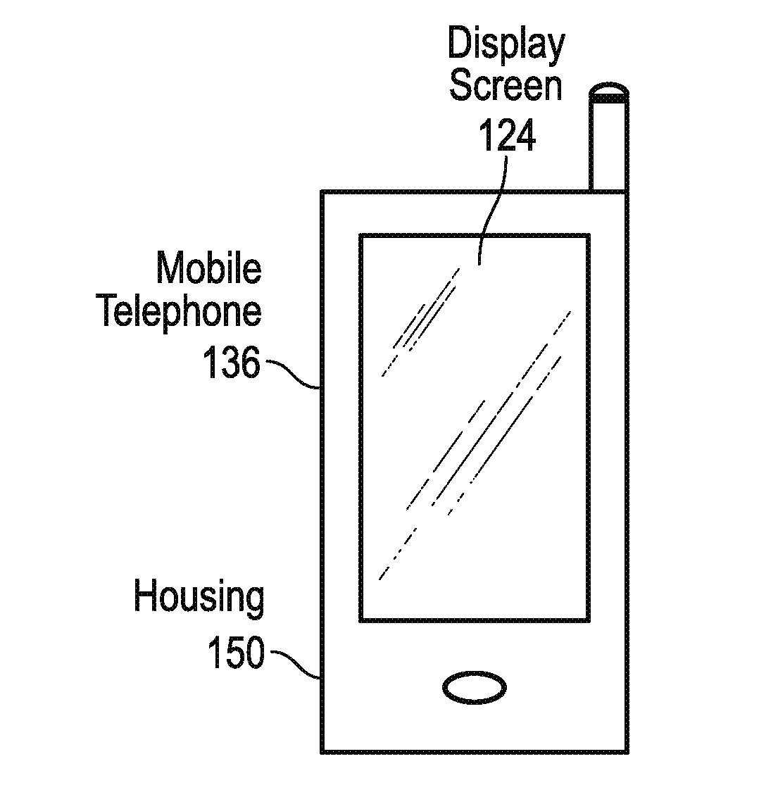
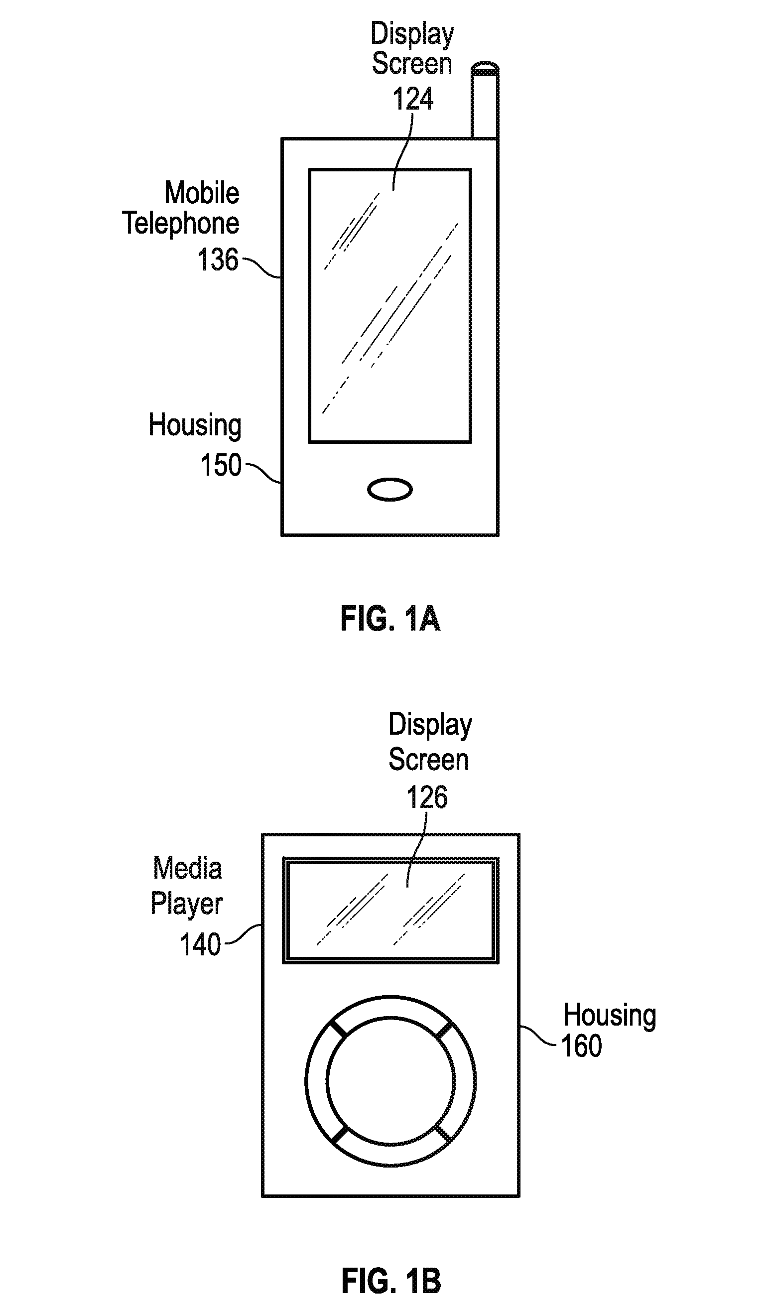
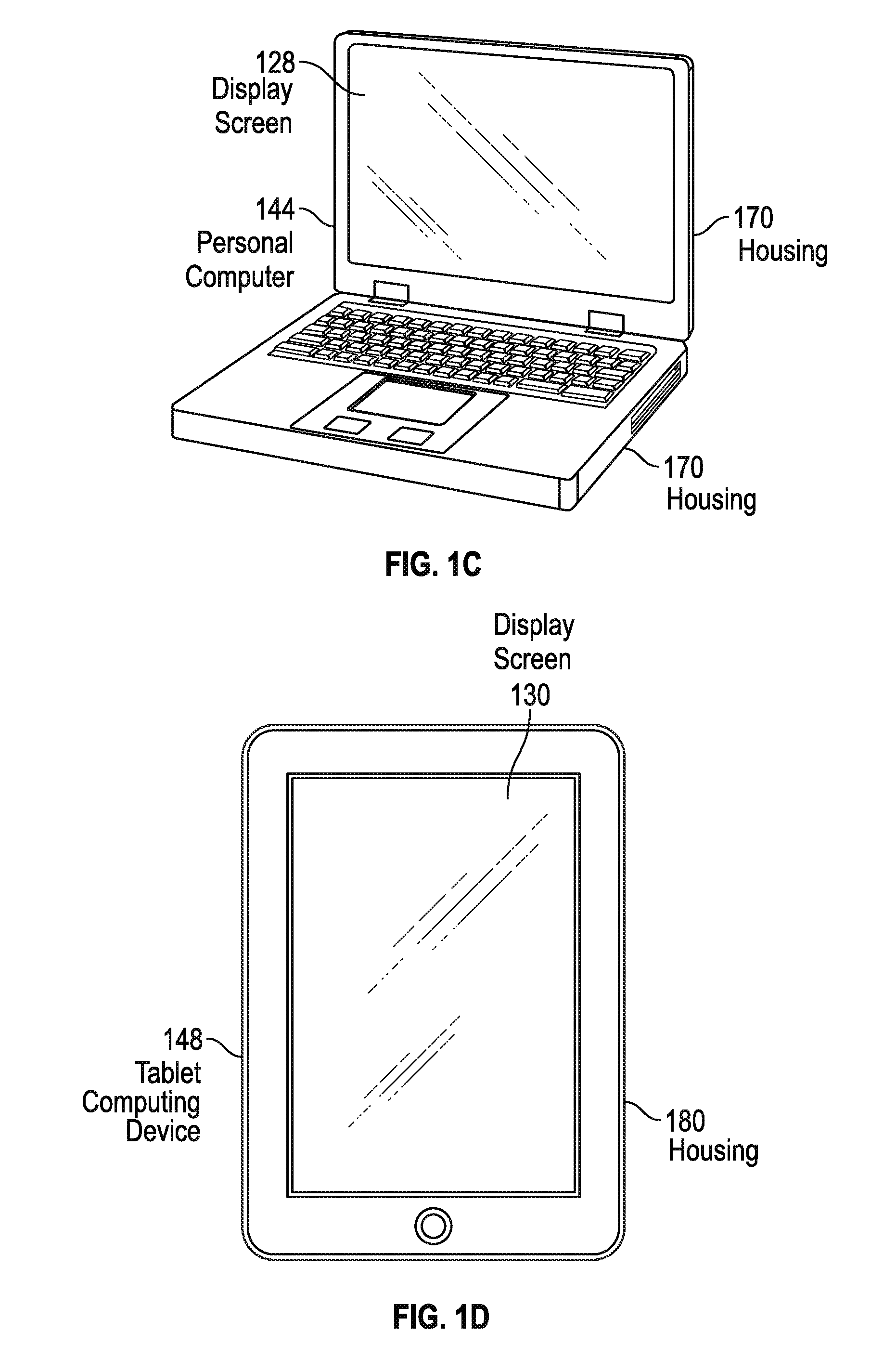
[0017]This relates to multi-layer thin film coatings for electrical, mechanical, and optical components and subsystems in a portable electronic device assembled using System-in-Package (SiP) technology. The multi-layer thin film coatings can be used for radio-frequency shielding and / or magnetic shielding. The multi-layer thin film coatings can shield components such as integrated circuits that operate in radio-frequency bands (e.g., transceiver integrated circuits, memory circuits and other circuits). Components can also include circuitry formed from one or more discrete components such as inductors, capacitors, resistors, switches, etc. The components that are ...


PUM

PropertyMeasurementUnit
Thicknessaaaaaaaaaa
Thicknessaaaaaaaaaa
Thicknessaaaaaaaaaa

Abstract

A portable electronic device packaged into a System-in-Package assembly is disclosed. The portable electronic device can include a substrate and a plurality of components mounted on the substrate and included in one or more subsystems. Interference between subsystems or from external sources can be reduced or eliminated by disposing an insulating layer over the components, forming narrow trenches between subsystems, and depositing one or more layers of a multi-layer thin film stack on the insulating layer and filling the trenches. In some examples, the multi-layer thin film stack can include an adhesion layer, a shielding layer, a protection layer, and a cosmetic layer. In some examples, the multi-layer thin film stack can include multi-functional layers such as a protection and cosmetic layer.

Description

FIELD[0001]This relates generally to mitigating interference and, more particularly, to thin film coatings to help provide electromagnetic shielding, adhesion to underlying layers, enhanced aesthetic appeal, and resistance to degradation or discoloration in System-In-Package assemblies in compact portable electronic devices.BACKGROUND[0002]Compact portable electronic devices are becoming increasingly popular. Examples of compact portable electronic devices include laptop computers, tablet computing devices, cellular telephones, media players, gaming devices, handheld devices, miniature devices such as pendant and wearable devices, and other devices. It is generally desirable to reduce both internal and external interference of the components in the compact portable electronic devices. The interference can be reduced or eliminated using electromagnetic shielding. For example, some electronic devices include radio-frequency transceiver circuits that are susceptible to radio-frequency ...

Claims


Application Information

Patent Timeline
IPC IPC(8): H05K1/02H05K3/28H05K3/30H05K1/18H05K9/00
CPCH05K1/0216H05K1/18H05K3/284H05K3/30H05K9/0081H05K1/0218H05K9/00H05K2201/09972H05K2201/10371H05K2203/1322H01L2924/3025Y10T29/49146H05K2201/0715
Inventor CHEN, YANFENGPENNATHUR, SHANKAR S.
Owner APPLE INC
Why Eureka
Try Eureka