Array substrate and manufacturing method thereof, and display apparatus
a technology applied in the field of array substrate and manufacturing method thereof, can solve the problems of poor display on the display apparatus, high production cost, etc., and achieve the effect of improving the display quality
- Summary
- Abstract
- Description
- Claims
- Application Information
AI Technical Summary
Benefits of technology
Problems solved by technology
Method used
Image
Examples
embodiment 1
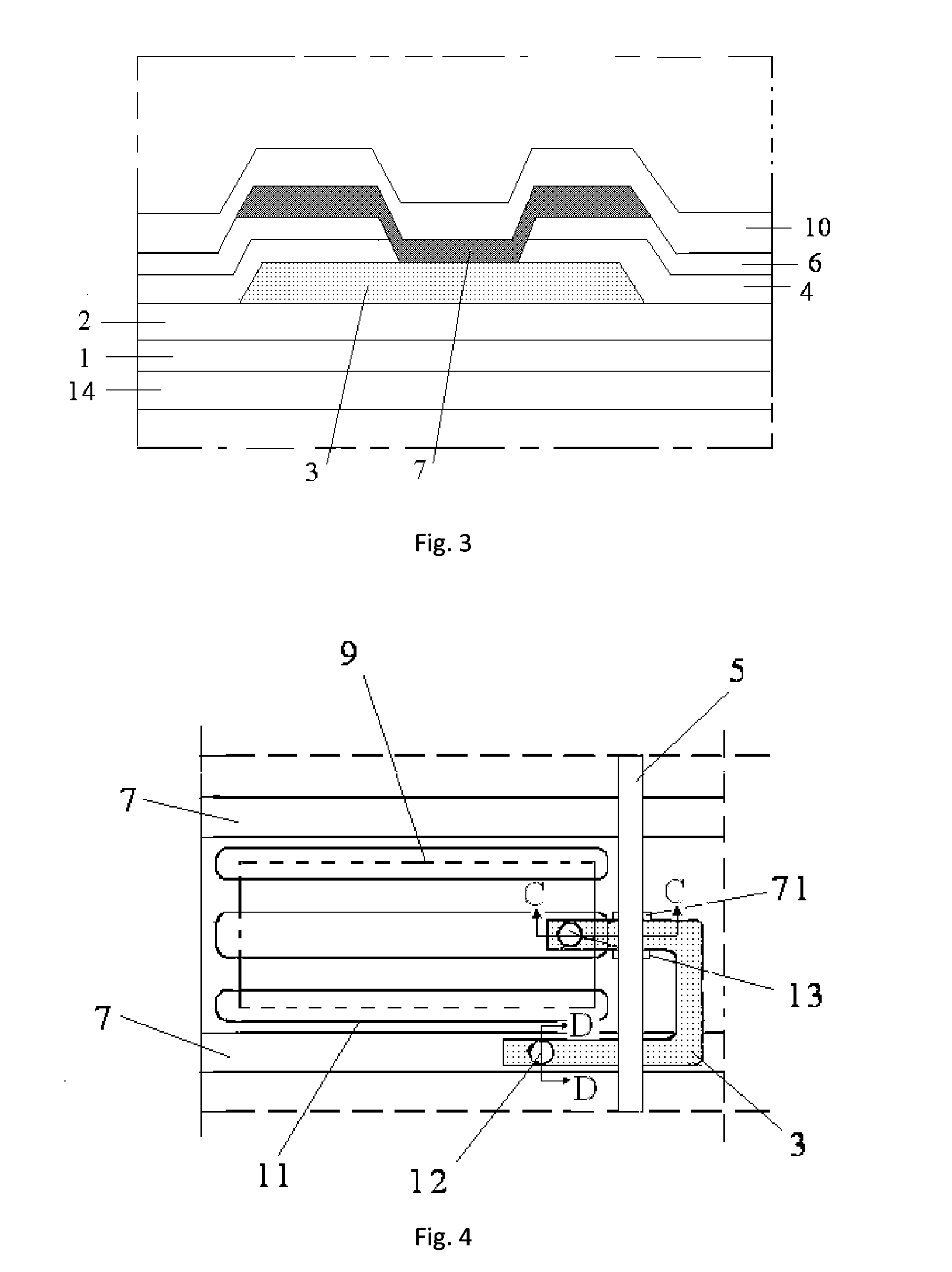
[0035]The present embodiment provides a manufacturing method of an array substrate. Referring to FIGS. 4-6, the manufacturing method comprises the following steps.
[0036]S1, depositing a data line metal layer on a substrate 14 by sputtering, thermal evaporation method, or other film forming methods, and forming a pattern of a data line 7 by a patterning process. The substrate 14 may be a glass substrate or other types of transparent substrate, and the data line metal layer may be formed of one of chromium (Cr), molybdenum (Mo), aluminum (Al), copper (Cu), tungsten (W), neodymium (Nd), or formed of an alloy of them. Moreover, the data line metal layer may be of one layer or more than one layers.
[0037]S2, forming a semiconductor layer on the substrate 14 formed with the data line 7 thereon, and forming a pattern of an active layer 3 by a patterning process, wherein the data line 7 is connected with the active layer 3.
[0038]The step S2 further comprises: depositing a polycrystalline sil...
embodiment 2
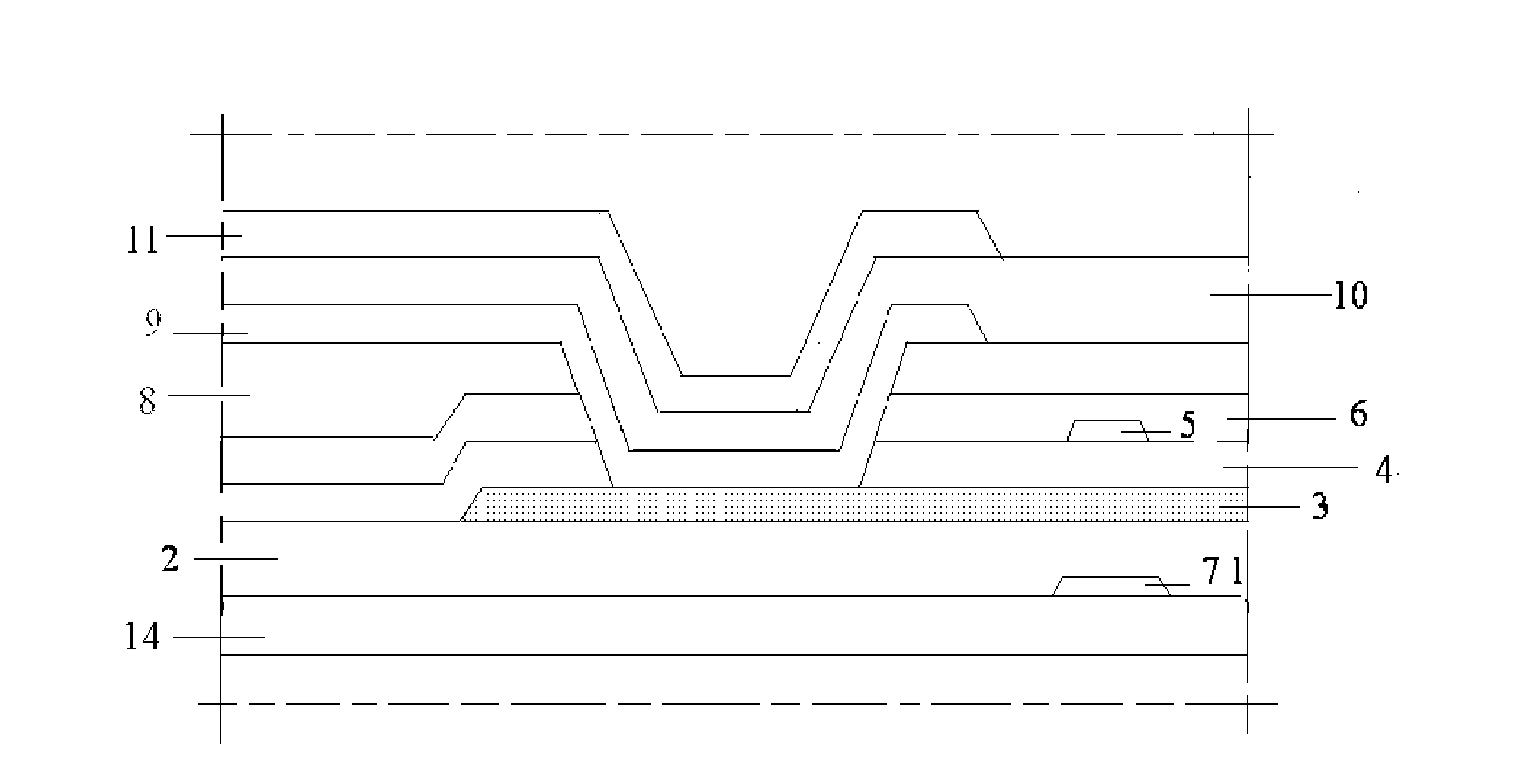
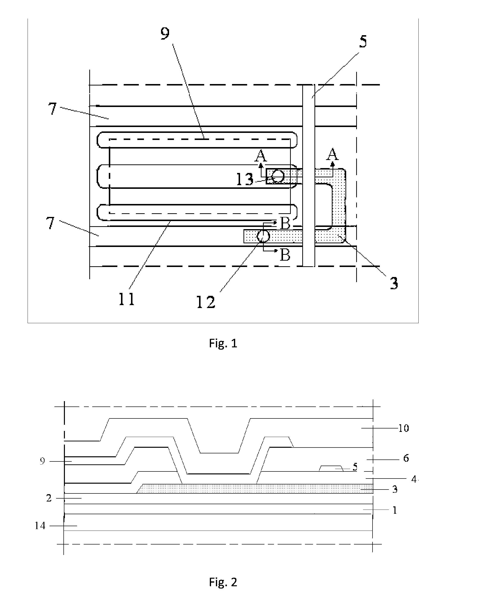
[0058]The present embodiment provides an array substrate. As shown in FIG. 4 to FIG. 8, the array substrate comprises a data line 7 and an active layer 3, wherein the data line 7 is below the active layer 3, and the data line 7 is connected with the active layer 3. Of course, the array substrate further comprises some known structures such as a gate line 5, a pixel electrode and so on, which are not described here.
[0059]The array substrate further comprises a pattern 71 of a shield metal for shielding the active region of the active layer 3, and the pattern 71 of the shield metal is below the active layer 3. As the active layer 3 is a semiconductor layer formed of polycrystalline silicon, and the semiconductor material is photosensitive, when it is irradiated by light (such as light from a backlight module), a leakage current may be generated therein, which influences performances of the active layer 3, and there may be adverse impacts on the performances of the thin film transistor...
PUM
 Abstract
Description
Claims
Application Information


