

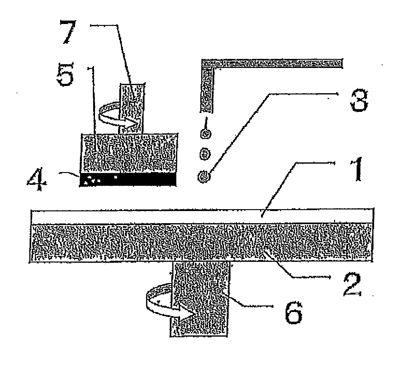
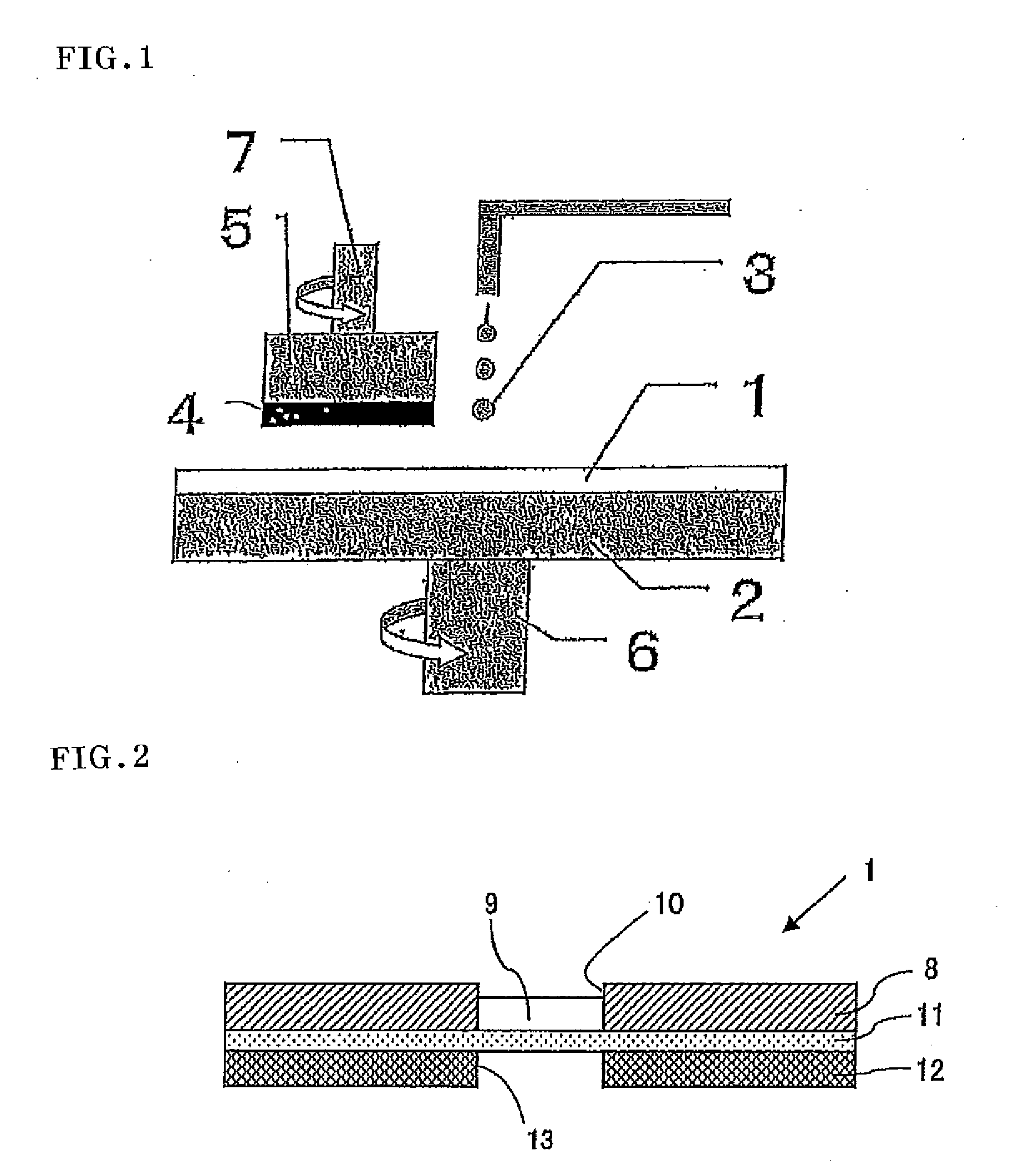
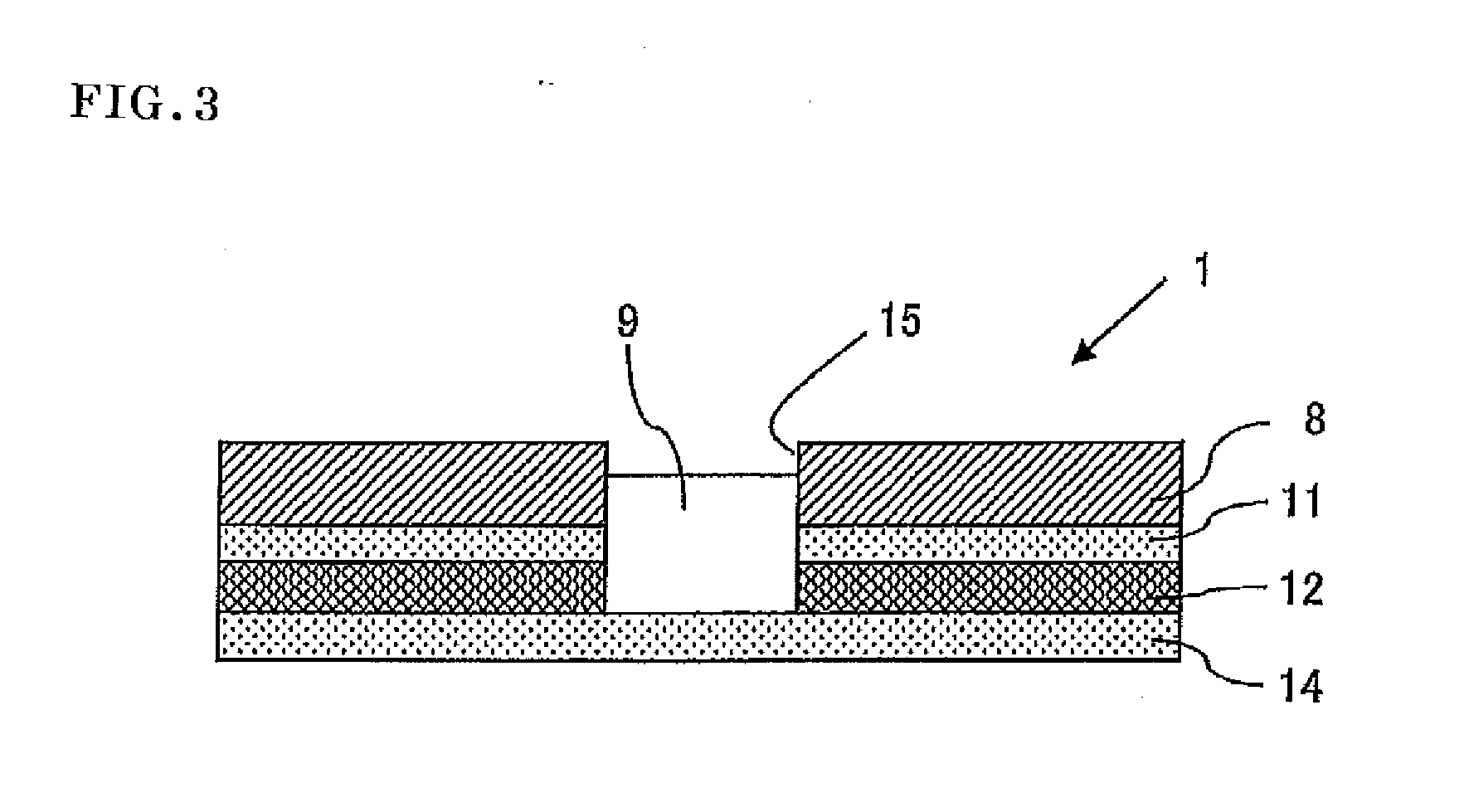
Multilayer polishing pad
a polishing pad and multi-layer technology, applied in the direction of lapping tools, electrical equipment, metal-working equipment, etc., can solve the problems of easy delamination between the polishing layer, the durability of the double-sided tape can decrease, and the wafer surface can be easily delaminated, so as to resist delamination
- Summary
- Abstract
- Description
- Claims
- Application Information
AI Technical Summary
Benefits of technology
Problems solved by technology
Method used
Image

Examples
example 1
[0129](Preparation of Polishing Layer)
[0130]To a vessel were added 1,229 parts by weight of toluene diisocyanate (a mixture of 2,4-diisocyanate / 2,6-diisocyanate=80 / 20), 272 parts by weight of 4,4′-dicyclohexylmethane diisocyanate, 1,901 parts by weight of polytetramethylene ether glycol with a number average molecular weight of 1,018, and 198 parts by weight of diethylene glycol, and allowed to react at 70° C. for 4 hours, so that an isocyanate-terminated prepolymer was obtained.
[0131]To a polymerization vessel were added 100 parts by weight of the prepolymer and 3 parts by weight of a silicone surfactant (SH-192 manufactured by Dow Corning Toray Co., Ltd.) and mixed. The mixture was adjusted to 80° C. and degassed under reduced pressure. Subsequently, the reaction system was vigorously stirred for about 4 minutes with a stirring blade at a rotational speed of 900 rpm so that air bubbles were incorporated into the reaction system. Thereto was added 26 parts by weight of MOCA (CUAMIN...
example 2
[0135]A multilayer polishing pad was prepared in the same manner as in Example 1, except that circular holes (1.6 mm in diameter×10 mm in pitch) were formed in a square lattice shape on the adhesive layer.
example 3
[0136]A multilayer polishing pad was prepared in the same manner as in Example 1, except that circular holes (8 mm in diameter×12 mm in pitch) were formed in a square lattice shape on the adhesive layer.
PUM
 Abstract
Description
Claims
Application Information