Imaging device, monitoring device, and electronic appliance

a monitoring device and imaging device technology, applied in the field of imaging devices, can solve the problems of a/d data conversion and a large amount of power consumption, and achieve the effect of low power consumption

Active Publication Date: 2015-11-19
SEMICON ENERGY LAB CO LTD
View PDF7 Cites 33 Cited by
  • Summary
  • Abstract
  • Description
  • Claims
  • Application Information

AI Technical Summary

Benefits of technology

[0020]According to one embodiment of the present invention, an imaging device

Problems solved by technology

Therefore, to generate the trigger signal, a vast amount of power is consumed by A/D conversion of the data read out from the CMOS image sensor, data transfer for taking a large

Method used


Image

  • Imaging device, monitoring device, and electronic appliance
  • Imaging device, monitoring device, and electronic appliance
  • Imaging device, monitoring device, and electronic appliance

Examples


embodiment 1

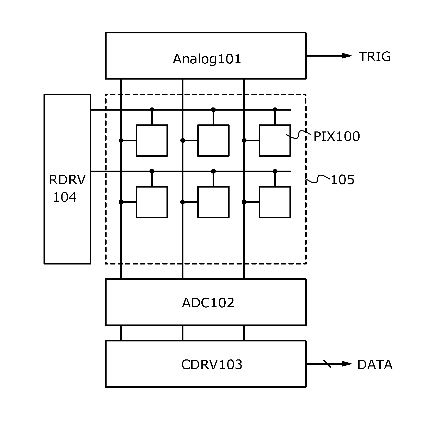
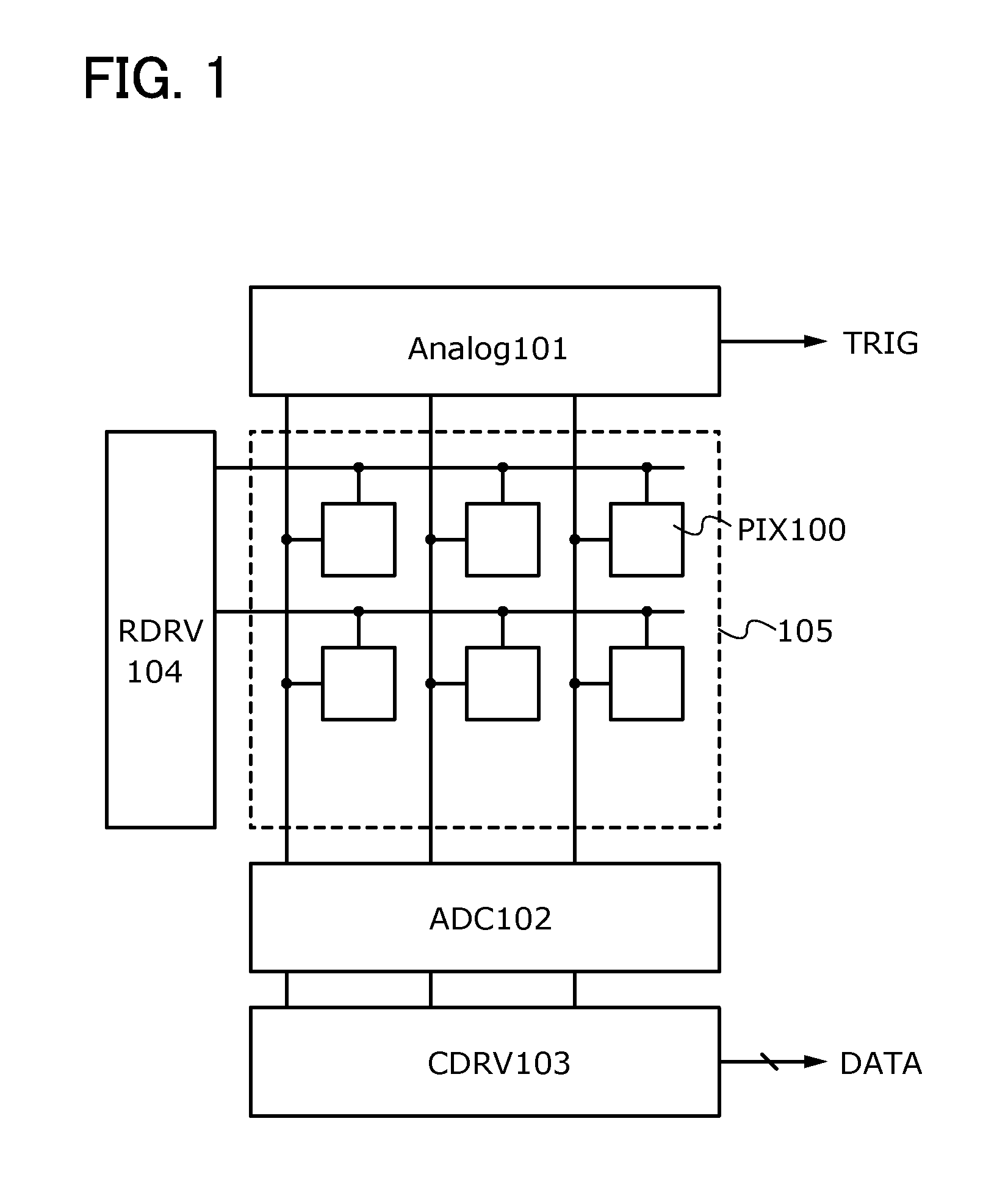
[0052]A configuration of an imaging device of one embodiment of the present invention is described with reference to FIG. 1. The imaging device of one embodiment of the present invention includes a pixel portion 105 including a plurality of pixels 100 (PIX 100) arranged in matrix, an analog processing circuit 101 (Analog 101), an A / D converter circuit 102 (ADC 102), which is a digital processing circuit, a column driver 103 (CDRV 103), and a row driver 104 (RDRV 104).

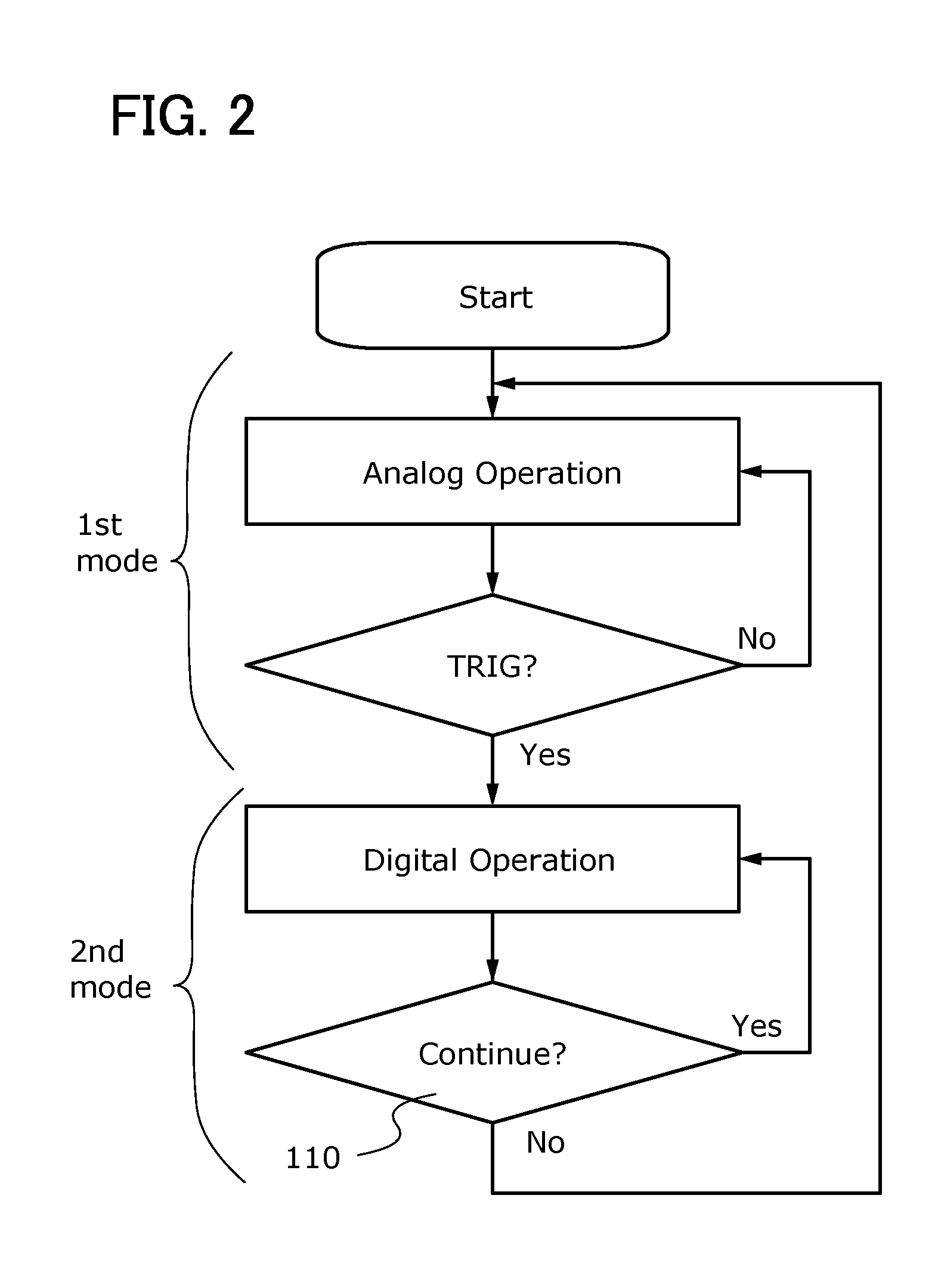
[0053]The pixels 100 each include a photodiode having a function of a photoelectric conversion element, and at least one transistor. The analog processing circuit 101 executes analog data processing on imaging data which is analog data output from each pixel 100. Specifically, the analog processing circuit 101 executes a sum-of-absolute-difference operation on imaging data output from each pixel 100. In the case where the obtained result of the operation is different from a predetermined value, a trigger signal (represe...

embodiment 2

[0061]A configuration of the pixel 100 included in the imaging device of one embodiment of the present invention is described with reference to FIG. 4A. The pixel 100 includes a transistor 111, a transistor 112, a transistor 113, a transistor 114, a transistor 115, a capacitor 121, a capacitor 122, and a photodiode 123. The pixel 100 is supplied with potentials from a power supply line VPD, a power supply line VPR, a power supply line VC, a power supply line VFR, and a power supply line VO; and supplied with control signals from a signal line TX, a signal line PR, a signal line FR, and a signal line SEL. Imaging data of the pixel 100 is output to a signal line OUT. Charge corresponding to the imaging data is accumulated in a charge retention node FD1. Here, the capacitance value of the capacitor 121 is preferably larger than the total capacitance value of the capacitor 122 and the gate capacitance of the transistor 114.

[0062]A gate of the transistor 111 is electrically connected to ...

embodiment 3

[0080]A configuration example of the analog processing circuit included in the imaging device of one embodiment of the present invention is described with reference to FIG. 6. The analog processing circuit includes subtraction circuits SUB[1] to SUB[n], absolute value circuits ABS[1] to ABS[n], and an adder circuit SUM.

[0081]The subtraction circuits SUB[1] to SUB[n] perform subtraction between potentials of signal lines OUT[1] to OUT[n] of pixels and a reference potential VREF, respectively. The reference potential VREF can be generated by providing a dummy circuit equivalent to the pixel 100 and using the potential of its signal line OUT when the potential of its charge retention node FD1 is VFR. The subtraction circuits SUB[1] to SUB[n] each include an OP amplifier OP0 and resistors R01 to R04. Here, in the subtraction circuit SUB[1], the potential of the signal line OUT and the potential of VREF are represented as V10 and V20, respectively. In addition, the resistance values of t...


PUM


Abstract

An imaging device capable of detecting differences with low power consumption is provided. The imaging device includes a pixel including a photoelectric conversion element and a transistor; an analog processing circuit; and a digital processing circuit. The imaging device is operated in a first mode and a second mode. In the first mode, the analog processing circuit detects a difference between first imaging data taken by the pixel and second imaging data taken by the pixel and generates a trigger signal on the basis of the value of the difference. In the second mode, the digital processing circuit converts third imaging data taken by the pixel into digital data. Switching from the first mode to the second mode is performed on the basis of the trigger signal.

Description

BACKGROUND OF THE INVENTION[0001]1. Field of the Invention[0002]One embodiment of the present invention relates to an imaging device, a monitoring device, and an electronic appliance which have a function of taking an image.[0003]Note that one embodiment of the present invention is not limited to the above technical field. The technical field of one embodiment of the invention disclosed in this specification and the like relates to an object, a method, or a manufacturing method. In addition, one embodiment of the present invention relates to a process, a machine, manufacture, or a composition of matter. Specifically, examples of the technical field of one embodiment of the present invention disclosed in this specification include a semiconductor device, a display device, a light-emitting device, a power storage device, a memory device, a method for driving any of them, and a method for manufacturing any of them.[0004]2. Description of the Related Art[0005]Imaging devices are normall...

Claims


Application Information

Patent Timeline
IPC IPC(8): G08B13/196H04N5/3745H04N5/232
CPCG08B13/19602H04N5/37455H04N5/23245G08B13/19604H04N23/667H04N25/771H04N25/75H04N7/18G08B13/196H04N25/77H04N25/772
Inventor KUROKAWA, YOSHIYUKI
Owner SEMICON ENERGY LAB CO LTD
Why Eureka
Try Eureka