Semiconductor device and method for manufacturing same

a technology of semiconductor devices and semiconductor devices, which is applied in the direction of semiconductor devices, basic electric elements, electrical equipment, etc., can solve the problems of dielectric breakdown of gate insulating films on the bottom of trenches, and achieve the effect of increasing on-resistance and reducing electric field concentration

Active Publication Date: 2015-11-19
PANASONIC INTELLECTUAL PROPERTY MANAGEMENT CO LTD
View PDF0 Cites 20 Cited by
  • Summary
  • Abstract
  • Description
  • Claims
  • Application Information

AI Technical Summary

Benefits of technology

[0017]According to the semiconductor device and the manufacturing method thereof, the impurity region can be formed on the bottom of the trench without misalignment. It is thus possible to reduce concentration of electric field and increase in on-resistance which can be caused by the misalignment.

Problems solved by technology

In the vertical MOSFET thus configured, when a high voltage is applied between the source and drain, concentration of electric field is likely to occur on the bottom of the trench, which causes a dielectric breakdown in the gate insulating film on the bottom of the trench.

Method used


Image

  • Semiconductor device and method for manufacturing same
  • Semiconductor device and method for manufacturing same
  • Semiconductor device and method for manufacturing same

Examples


first embodiment

[0048]—Structure of Semiconductor Device—

[0049]An illustrative semiconductor device 100 according to a first embodiment of the present disclosure and a manufacturing method thereof will be described below with reference to the drawings.

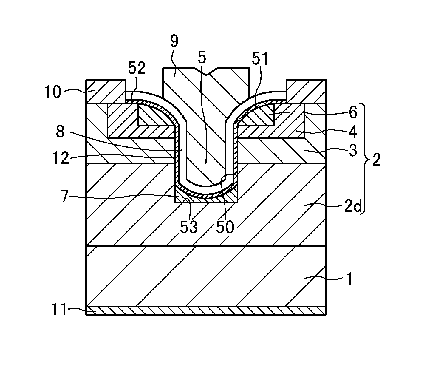
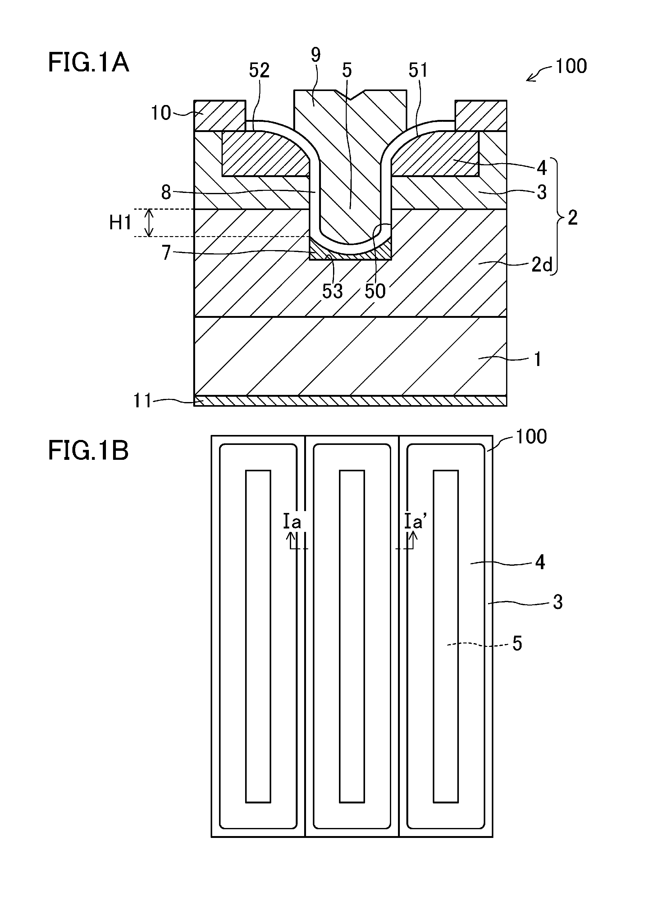
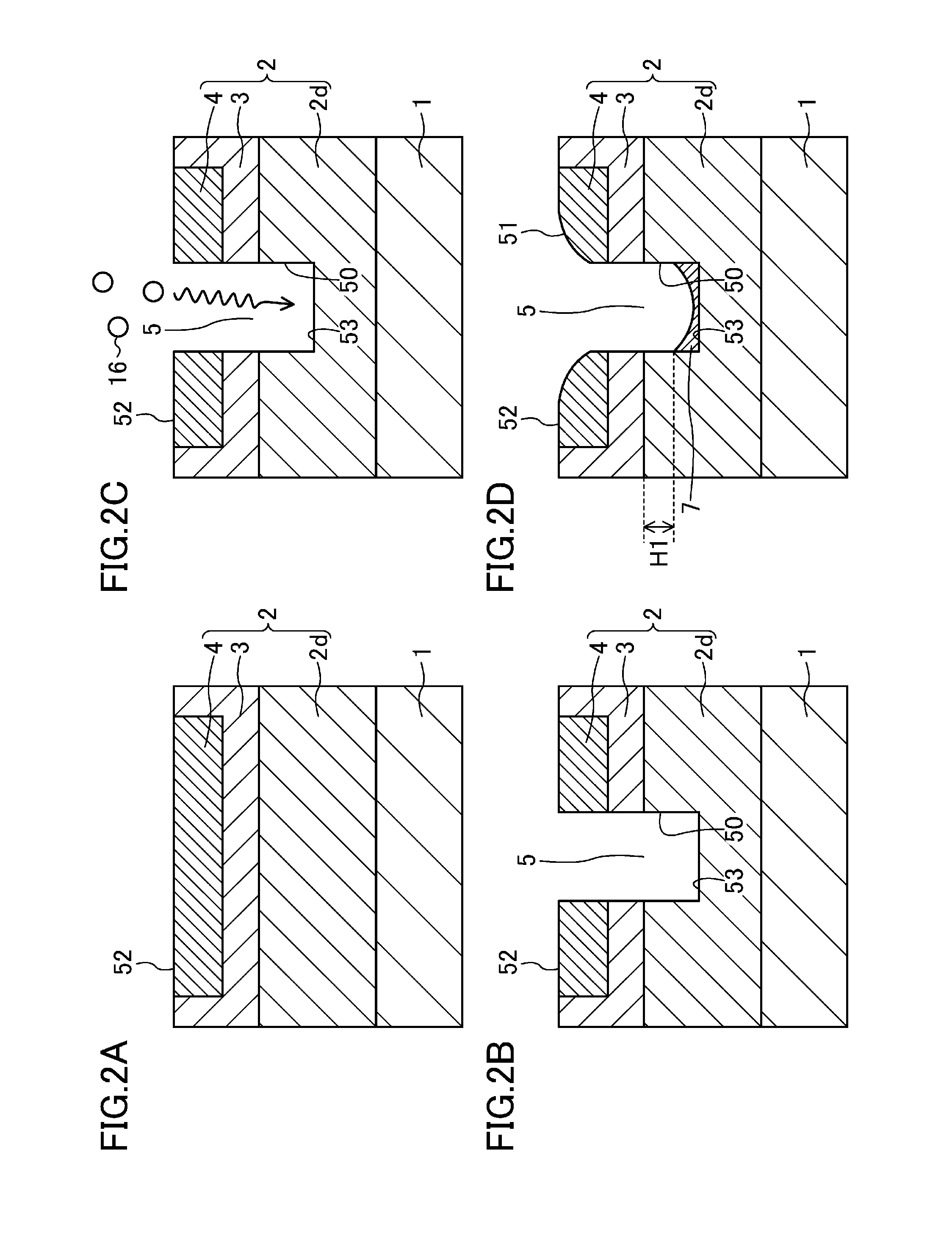
[0050]For example, the semiconductor device 100 includes a plurality of unit cells each of which is a SiC-metal-insulator-semiconductor field-effect transistor (SiC-MISFET) having a trench gate structure.

[0051]FIG. 1A schematically illustrates a cross-sectional configuration of one of the plurality of unit cells included in the semiconductor device 100. FIG. 1B schematically illustrates an exemplary configuration of the semiconductor device 100 viewed from above, specifically, the surfaces of silicon carbide layers of the plurality of unit cells (three unit cells in this embodiment). FIG. 1A is the cross-sectional view taken along the line Ia-Ia′ in FIG. 1B. FIG. 1B illustrates an arrangement of body regions 3, source regions 4, and trenches 5 while o...

second embodiment

[0136]—Structure of Semiconductor Device—

[0137]An illustrative semiconductor device 100a according to a second embodiment of the present disclosure and a manufacturing method of the semiconductor device 100a will be described below with reference to the drawings.

[0138]For example, the semiconductor device is a silicon carbide semiconductor device, and specifically, includes a plurality of unit cells each of which is a SiC-metal-insulator-semiconductor field-effect transistor (SiC-MISFET) having a trench gate structure.

[0139]FIG. 9A schematically illustrates a cross-sectional configuration of one of the plurality of the unit cells included in the semiconductor device 100a. FIG. 9B schematically illustrates an exemplary configuration of the semiconductor device 100a viewed from above, specifically, the surfaces of silicon carbide layers of the plurality of unit cells (three unit cells in this case). FIG. 9A is the cross-sectional view taken along the line Xia-XIa′ in FIG. 9B. FIG. 9B ...


PUM


Abstract

A method for manufacturing a semiconductor device includes the steps of: forming, on a principal face of a substrate, a semiconductor layer including a first semiconductor region of a first conductivity type; and forming, in the semiconductor layer, a trench having a bottom located in the first semiconductor region. The method further includes a step of forming a trench bottom impurity region being of a second conductivity type and covering the bottom of the trench by performing annealing to cause part of the semiconductor layer corresponding to an upper corner portion of the trench to move to be placed on the bottom of the trench.

Description

TECHNICAL FIELD[0001]The present disclosure relates to semiconductor devices and manufacturing method of the semiconductor devices, and in particular, to semiconductor devices (power semiconductor devices) capable of withstanding a high voltage and a large current.BACKGROUND ART[0002]Silicon carbide (SiC), of which the band gap and the dielectric breakdown voltage strength are greater than those of silicon (Si), is a semiconductor material which is expected to be applied to next-generation low-loss power devices, for example. SiC exists in various polytypes such as 3C—SiC which is a cubic system, 6H—SiC and 4H—SiC which are hexagonal systems. Among the polytypes, 4H—SiC is generally used for producing silicon carbide semiconductor devices.[0003]A typical power device including SiC and serving as a switching element is a field effect transistor such as a metal insulator semiconductor field effect transistor (hereinafter referred to as a “MISFET”) or a metal semiconductor field effect...

Claims


Application Information

Patent Timeline
Patent Type & Authority Applications(United States)
IPC IPC(8): H01L29/78H01L29/66H01L21/306H01L21/02H01L29/16H01L21/04H01L21/223H01L21/324H01L29/417
CPCH01L29/7813H01L21/324H01L29/66734H01L21/30604H01L29/41741H01L21/02529H01L29/66068H01L21/0455H01L21/223H01L21/02378H01L29/1608H01L21/0475H01L21/049H01L29/0619H01L29/0623H01L29/0696H01L29/4236H01L29/6606H01L29/7828H01L29/861H01L29/872H01L21/0243H01L21/02576H01L21/0262H01L21/302H01L21/3065H01L21/3247
Inventor KIYOSAWA, TSUTOMUKUDOU, CHIAKITOMITA, YUKI
Owner PANASONIC INTELLECTUAL PROPERTY MANAGEMENT CO LTD
Why Eureka
Try Eureka