Nitride semiconductor light emitting device

a technology of nitride semiconductors and light emitting devices, which is applied in the direction of semiconductor lasers, semiconductor devices, electrical devices, etc., can solve the problems of inconvenient short-livedness, low light output, and large size, and achieve the effect of improving the light emission efficiency of nitride semiconductor deep ultraviolet light emitting devices

Inactive Publication Date: 2016-01-07
STANLEY ELECTRIC CO LTD
View PDF36 Cites 23 Cited by
  • Summary
  • Abstract
  • Description
  • Claims
  • Application Information

AI Technical Summary

Benefits of technology

[0030]According to the present invention, electrons in nitride semiconductor deep ultraviolet light emitting devices whose emission wavelength is 300 nm or less can be prevented from overflowing, and thus it is possible to improve the light emission efficiency of the nitride semiconductor deep ultraviolet light emitting devices.

Problems solved by technology

There are inconveniences of shortlivedness, large size and so on in these gas discharge lamps.
However, there are problems with light emitting devices employing semiconductors that light output is lower compared to that from gas discharge lamps such as heavy hydrogen-vapor lamps and mercury-vapor lamps; and the light emission efficiency is also low.
It is a cause of insufficient light output from semiconductor light emitting devices that in nitride semiconductor light emitting devices, the effective mass of electrons is smaller compared to holes, and the career density is high; thus, electrons cross over active layers (region), to overflow p-type layers, which results in their low light emission efficiency.
Such an overflow of electrons to p-type layers results in a further low light emission efficiency under the condition of high injection currents, and at the same time, heating values are increased.
As a result, light output has stopped increasing, and it becomes difficult to obtain light output corresponding to the amount of injected carriers.
The problem of an overflow of electrons to p-type layers in nitride semiconductor light emitting devices is not only with deep ultraviolet light emitting devices whose emission wavelength is 300 nm or less (for example, see Non Patent Literature 1).

Method used


Image

  • Nitride semiconductor light emitting device
  • Nitride semiconductor light emitting device
  • Nitride semiconductor light emitting device

Examples


examples 2 to 5

Example 2

[0150]A wafer including a plurality of the nitride semiconductor light emitting devices of stacked structures depicted in FIG. 1 was manufactured, and nitride semiconductor light emitting devices were cut out from the wafer. It is noted that the number of quantum wells in each active layer was three.

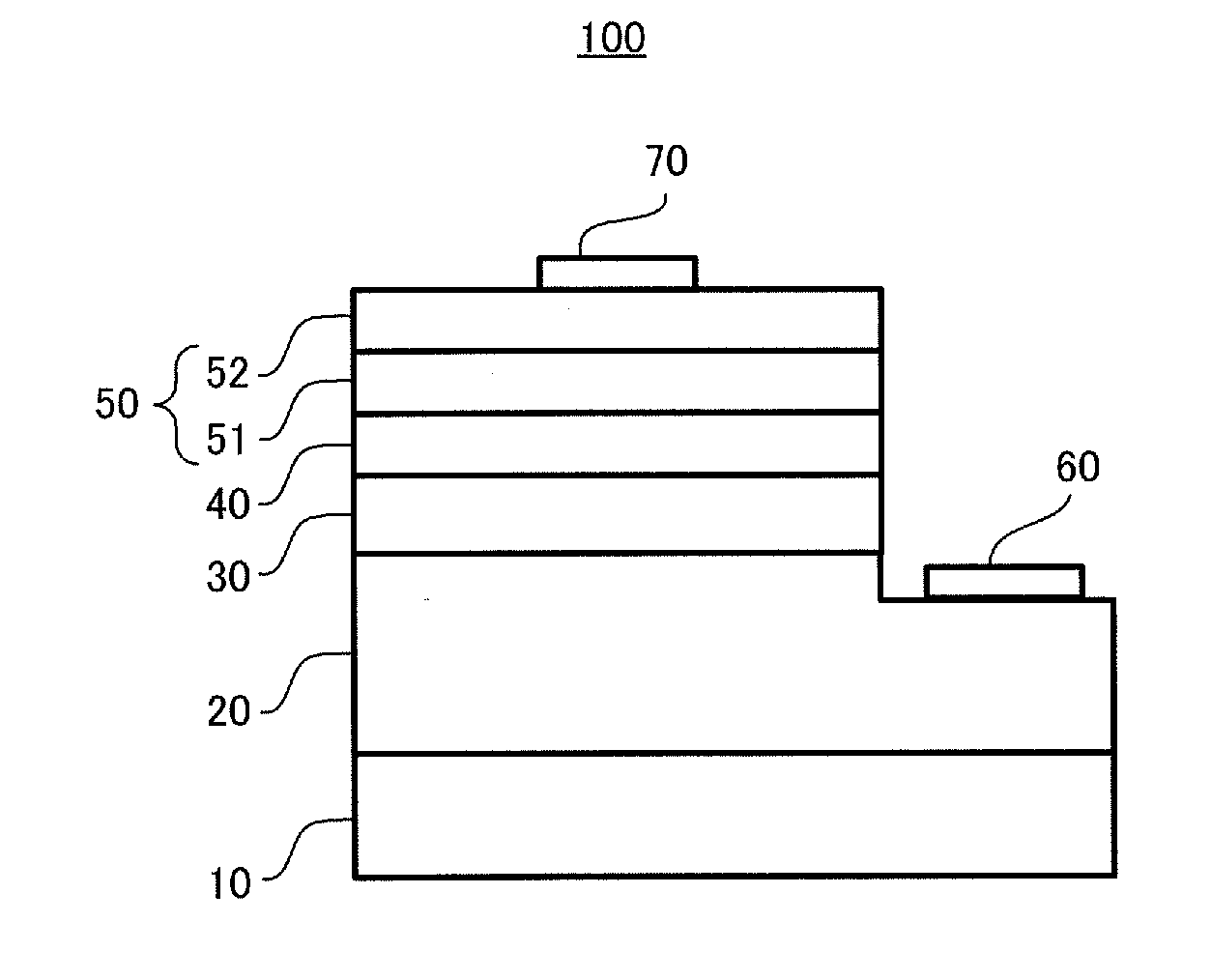
[0151]First, an Al0.75Ga0.25N layer of 1.0 μm in thickness where Si was doped (band gap: 5.23 eV, Si concentration: 1×1019 cm−3) was formed on a c-plane of the AlN substrate (10), which was 7 by 7 mm square and 500 μm in thickness, by MOCVD as the n-type layer (20).

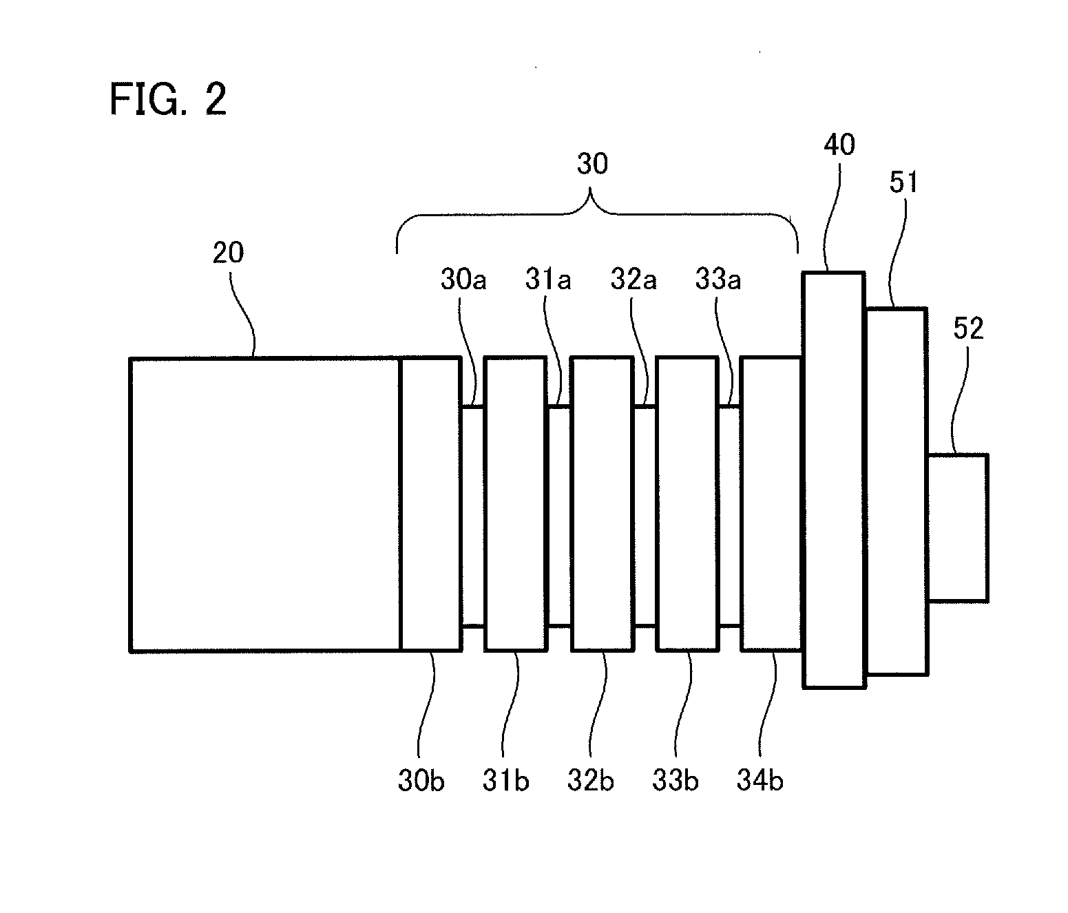
[0152]The active layer (30) having a quantum well structure that included three quantum wells was formed over the n-type layer (20) by composing four barrier layers where Si was doped (composition: Al0.75Ga0.25N, band gap: 5.23 eV, Si concentration: 1×1018 cm−3, and thickness: 7 nm) and three well layers (composition: Al0.5Ga. 5N, band gap: 4.55 eV, undoped, and thickness: 2 nm) so that the barrier layers and the well...

example 3

[0157]The nitride semiconductor wafer and nitride semiconductor light emitting device were manufactured with the same operation as Example 2 except that in Example 2, each barrier layer was changed to have the composition Al0.65Ga0.35N (band gap: 4.95 eV, Si concentration: 1×1018 cm−3). The obtained nitride semiconductor light emitting device had the emission wavelength of 267 inn when the current injection was 100 mA, and its external quantum efficiency was 2.3%.

example 4

[0158]The nitride semiconductor wafer and nitride semiconductor light emitting device were manufactured with the same operation as Example 3 except that in Example 3, the thickness of each well layer was changed from 2 nm to 4 nm. The obtained nitride semiconductor light emitting device had the emission wavelength of 270 nm when the current injection was 100 mA, and its external quantum efficiency was 2.7%.


PUM


Abstract

A nitride semiconductor deep ultraviolet light emitting device having a superior light emission efficiency is provided. A nitride semiconductor light emitting device having emission wavelength of 200 to 300 nm includes an n-type layer consisting of a single layer or a plurality of layers having different band gaps, a p-type layer consisting of a single layer or a plurality of layers having different band gaps, an active layer arranged between the n-type layer and the p-type layer, and an electron blocking layer having a band gap larger than any band gap of layers composing the active layer and the p-type layer. The p-type layer includes a first p-type layer having a band gap larger than a band gap of a first n-type layer which has a smallest band gap in the n-type layer. The electron blocking layer is arranged between the active layer and the first p-type layer.

Description

TECHNICAL FIELD[0001]The present invention relates to a novel deep ultraviolet light emitting device that employs a nitride semiconductor and whose emission wavelength is in the range of 200 to 300 nm.BACKGROUND ART[0002]Under present circumstances, gas discharge lamps using heavy hydrogen, mercury, or the like are used as deep ultraviolet light sources whose emission wavelength is 300 nm or less. There are inconveniences of shortlivedness, large size and so on in these gas discharge lamps. In addition, mercury is a substance on which more and more conventions are regulating activities. Thus, the realization of deep ultraviolet light emitting devices employing semiconductors that are possible to overcome these inconvenience and that are easy to be treated is awaited.[0003]However, there are problems with light emitting devices employing semiconductors that light output is lower compared to that from gas discharge lamps such as heavy hydrogen-vapor lamps and mercury-vapor lamps; and ...

Claims


Application Information

Patent Timeline
Patent Type & Authority Applications(United States)
IPC IPC(8): H01L33/06H01L33/00H01L33/14H01L33/32
CPCH01L33/06H01L33/0025H01L33/145H01L33/32H01L33/04H01S5/2009H01S5/34333
Inventor OBATA, TOSHIYUKI
Owner STANLEY ELECTRIC CO LTD
Why Eureka
Try Eureka