Nonvolatile memory device

a non-volatile memory and peripheral circuit technology, applied in semiconductor devices, semiconductor/solid-state device details, electrical apparatus, etc., can solve the problems of memory loss, synchronous dram (sdram) may lose stored data, etc., to achieve the effect of reducing the parasitic capacitance and resistance between transistors in the peripheral circuit of a non-volatile memory device, reducing the propagation delay in the peripheral circuit, and increasing the performance of the non-volatile memory

Active Publication Date: 2016-03-17
SAMSUNG ELECTRONICS CO LTD
View PDF0 Cites 13 Cited by
  • Summary
  • Abstract
  • Description
  • Claims
  • Application Information

AI Technical Summary

Benefits of technology

[0006]According to exemplary embodiments of the present inventive concept, parasitic capacitance and resistance between transistors in a peripheral circuit of a nonvolatile memory device may be reduced. Accordingly, propagation delay in the peripheral circuit may be reduced and a performance of the nonvolatile memory device may be increased.

Problems solved by technology

A volatile memory device such as a Static RAM (Static Random Access Memory), a Dynamic RAM (DRAM), or a Synchronous DRAM (SDRAM) may lose stored data when power to the memory is lost.

Method used


Image

  • Nonvolatile memory device
  • Nonvolatile memory device
  • Nonvolatile memory device

Examples


Embodiment Construction

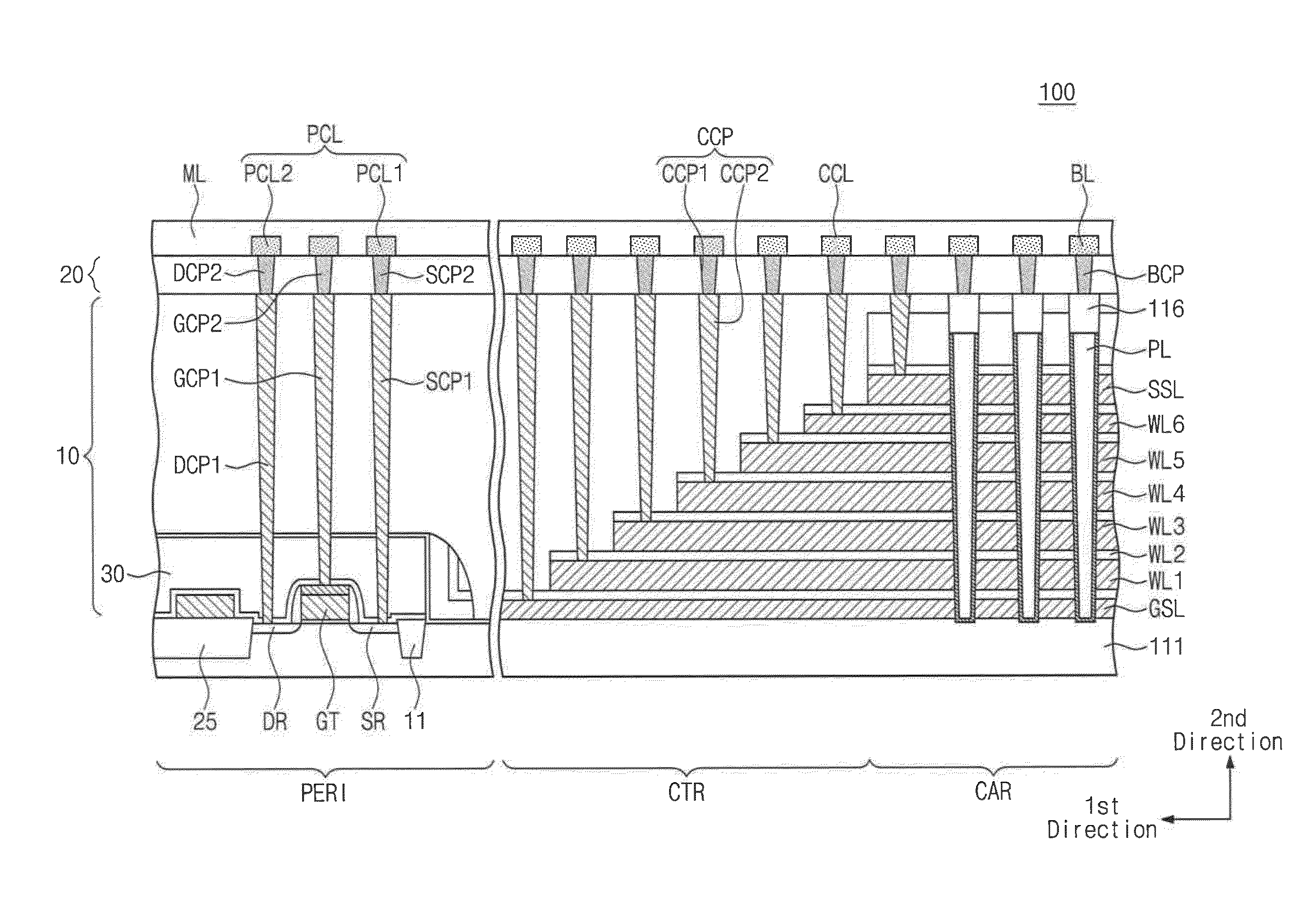
[0073]Exemplary embodiments of the present inventive concept are disclosed herein. However, specific structural and functional details disclosed herein may be merely representative and may be provided for purposes of describing exemplary embodiments of the present inventive concept. Exemplary embodiments of the present inventive concept may, however, be embodied in alternate forms and the present inventive concept should not be construed as limited to only the exemplary embodiments set forth herein.

[0074]Accordingly, exemplary embodiments of the present inventive concept are capable of various modifications and alternative forms. It should be understood that there is no intent to limit the exemplary embodiments of the present inventive concept to the particular forms disclosed, but to the contrary, exemplary embodiments of the present inventive concept are to cover all modifications, equivalents, and alternatives falling within the scope of exemplary embodiments of the present inven...


PUM


Abstract

A nonvolatile memory device includes a memory cell array and a peripheral circuit. The peripheral circuit is connected to the memory cell array through conductive lines and includes transistors. Each of the transistors is formed on the substrate and includes first and second regions and a gate electrode. In at least one of the transistors, the first region is connected to at least one of the conductive lines through first contact plugs extending in the direction perpendicular to the substrate, and second contact plugs extending in the direction perpendicular to the substrate. A contact area of each of the first contact plugs is different from a contact area of each of the second contact plugs.

Description

CROSS-REFERENCE TO RELATED APPLICATION[0001]This U.S. non-provisional patent application claims priority under 35 U.S.C. §119 to Korean Patent Application No. 10-2014-0122067 filed Sep. 15, 2014, in the Korean Intellectual Property Office, the disclosure of which is incorporated by reference herein in its entirety.TECHNICAL FIELD[0002]Exemplary embodiments of the present inventive concept relate to a semiconductor memory device, and more particularly, to a nonvolatile memory device.DISCUSSION OF RELATED ART[0003]A semiconductor memory device may include semiconductors, which include materials such as silicon (Si), germanium (Ge), gallium arsenide (GaAs), or indium phosphide (InP). Semiconductor memory devices may include volatile memory devices and nonvolatile memory devices.[0004]A volatile memory device such as a Static RAM (Static Random Access Memory), a Dynamic RAM (DRAM), or a Synchronous DRAM (SDRAM) may lose stored data when power to the memory is lost. A nonvolatile memory ...

Claims


Application Information

Patent Timeline
Patent Type & Authority Applications(United States)
IPC IPC(8): H01L27/115H01L23/528H01L23/535
CPCH01L27/11573H01L27/11582H01L23/535H01L27/1203H01L23/528H01L27/11578H01L27/11514H01L27/1157H10B43/50H10B43/40H10B43/35H10B43/27H10B43/20H10B53/20
Inventor SON, JAI-ICKKIM, SUNGHOON
Owner SAMSUNG ELECTRONICS CO LTD
Why Eureka
Try Eureka