

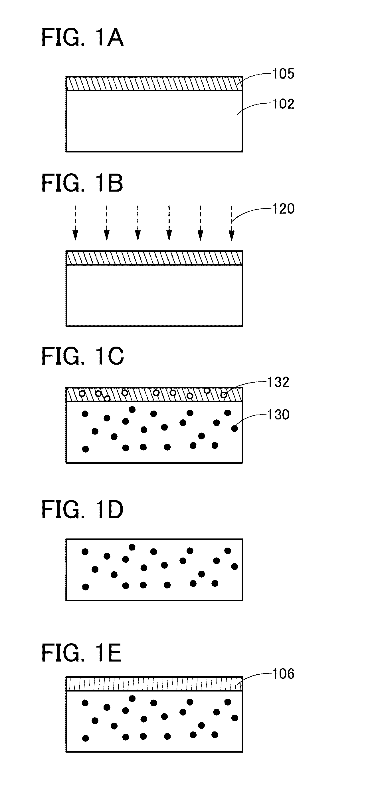
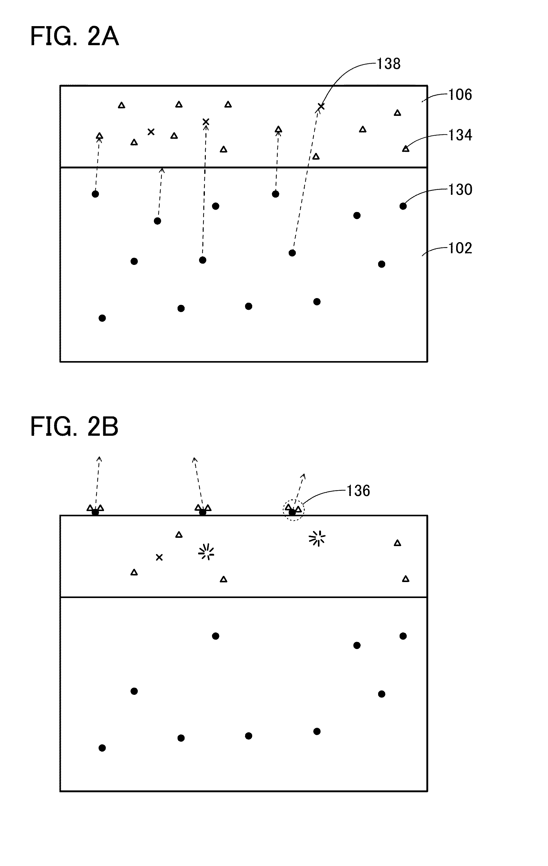
Method for manufacturing semiconductor device
a semiconductor and manufacturing technology, applied in semiconductor devices, diodes, electrical devices, etc., can solve the problems of small power consumption of display devices to which a transistor including an oxide semiconductor is applied, and achieve the effects of low defect density, excellent electrical characteristics, and low leakage curren
- Summary
- Abstract
- Description
- Claims
- Application Information
AI Technical Summary
Benefits of technology
Problems solved by technology
Method used
Image

Examples
configuration example 1
of Pixel
[0340]Each of the pixels 211 included in the imaging device 200 is formed with a plurality of subpixels 212, and each subpixel 212 is combined with a filter (color filter) which transmits light with a specific wavelength band, whereby data for achieving color image display can be obtained.
[0341]FIG. 23A is a plan view illustrating an example of the pixel 211 with which a color image is obtained. The pixel 211 illustrated in FIG. 23A includes the subpixel 212 provided with a color filter transmitting light with a red (R) wavelength band (also referred to as a “subpixel 212R”), the subpixel 212 provided with a color filter transmitting light with a green (G) wavelength band (also referred to as a “subpixel 212G”), and the subpixel 212 provided with a color filter transmitting light with a blue (B) wavelength band (also referred to as a “subpixel 212B”). The subpixels 212 can function as photosensors.
[0342]Each of the subpixels 212 (the subpixel 212R, the subpixel 212G, and the...
configuration example 2
of Pixel
[0356]An example of a pixel including a transistor using silicon and a transistor using an oxide semiconductor is described below.
[0357]FIGS. 25A and 25B are each a cross-sectional view of an element included in an imaging device. The imaging device illustrated in FIG. 25A includes a transistor 351 including silicon over a silicon substrate 300, transistors 352 and 353 which include an oxide semiconductor and are stacked over the transistor 351, and a photodiode 360 provided in a silicon substrate 300. The transistors and the photodiode 360 are electrically connected to various plugs 370 and wirings 371. In addition, the photodiode 360 includes an anode 361 and a cathode 362, and the anode 361 is electrically connected to the plug 370 through a low-resistance region 363.
[0358]The imaging device includes a layer 310 including the transistor 351 provided on the silicon substrate 300 and the photodiode 360 provided in the silicon substrate 300, a layer 320 which is in contact w...
PUM
 Abstract
Description
Claims
Application Information