TDI Sensor in a Darkfield System

a darkfield system and sensor technology, applied in the direction of image enhancement, instruments, image data processing, etc., can solve the problems of limiting the inspection speed required, the limit of the inspection sensitivity of the existing spot scanning technology, and the inability to increase the illumination photon number, so as to reduce the scattering of photons, increase the signal/background and signal/noise ratio, and reduce the effect of air scatter

Active Publication Date: 2016-04-07
KLA TENCOR TECH CORP
View PDF3 Cites 46 Cited by
  • Summary
  • Abstract
  • Description
  • Claims
  • Application Information

AI Technical Summary

Benefits of technology

[0010]In at least one embodiment of the present invention, a wafer scanning system includes imaging collection optics to collect scattered light. Imaging the illuminated wafer area onto a multi-pixel sensor results in each pixel receiving a fraction of the background signal, while the defect signal is imaged onto a much smaller number of pixels...

Problems solved by technology

Increasing the number of illumination photons is not an option because of the thermal damage threshold, above which the illumination photons begin to damage the surface.
Existing spot scanning technologies have reached the limit of inspection sensitivity.
Technologies i...

Method used


Image

  • TDI Sensor in a Darkfield System
  • TDI Sensor in a Darkfield System
  • TDI Sensor in a Darkfield System

Examples


Embodiment Construction

[0019]Reference will now be made in detail to the subject matter disclosed, which is illustrated in the accompanying drawings. The scope of the invention is limited only by the claims; numerous alternatives, modifications and equivalents are encompassed. For the purpose of clarity, technical material that is known in the technical fields related to the embodiments has not been described in detail to avoid unnecessarily obscuring the description.

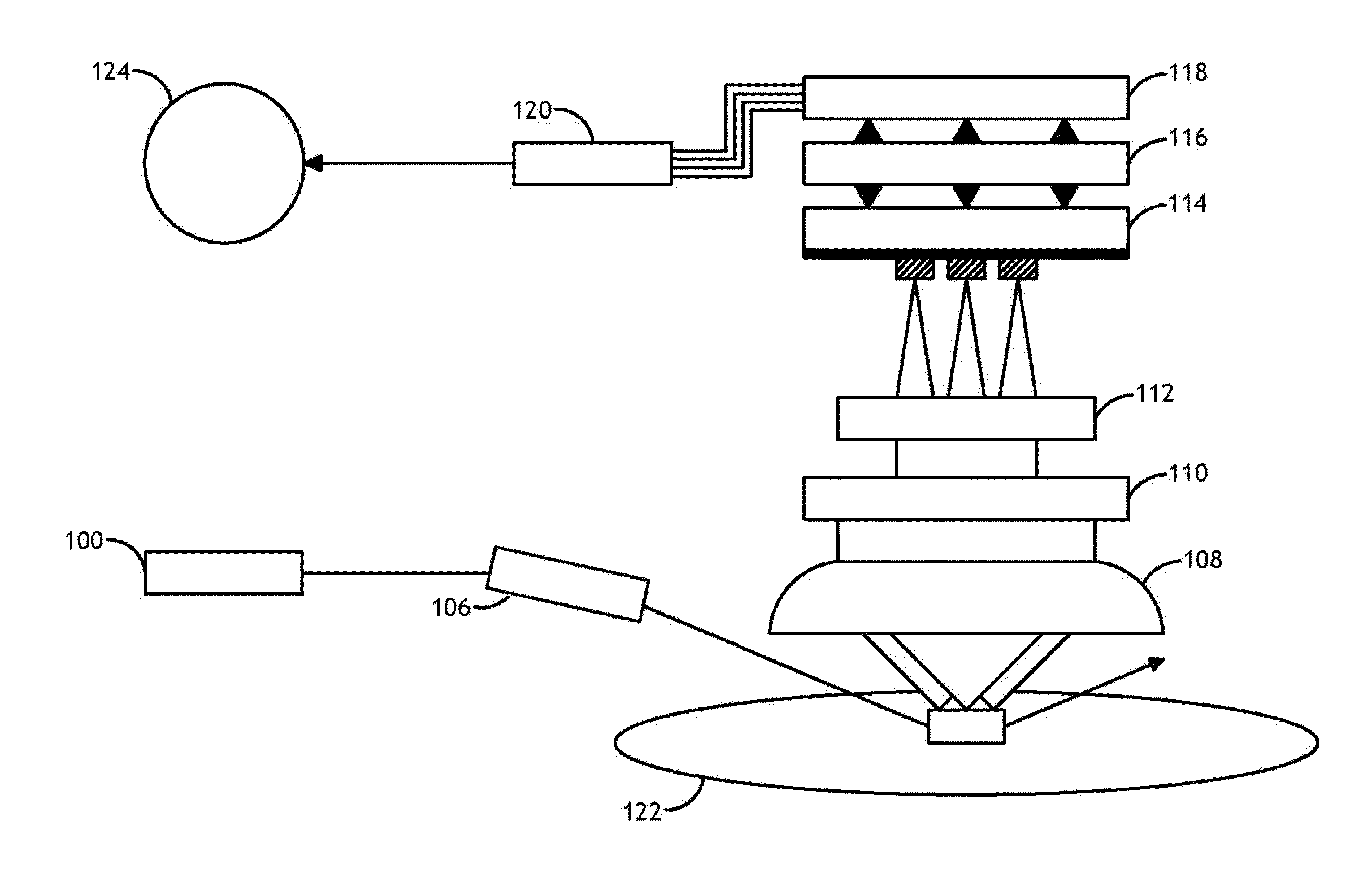
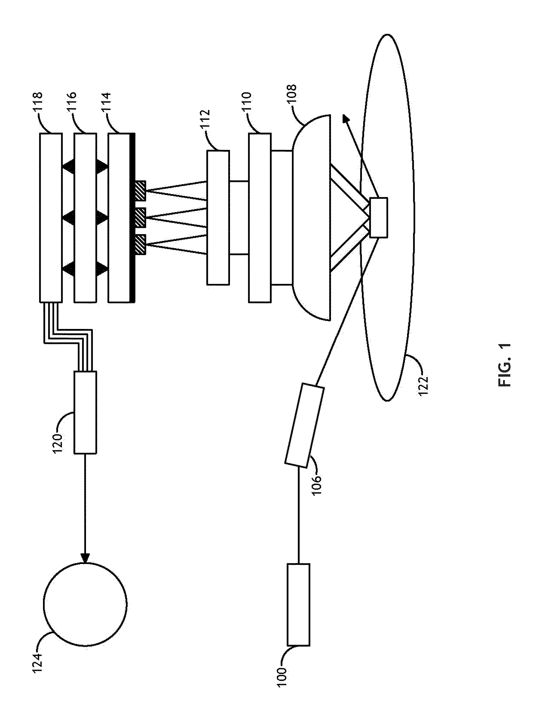
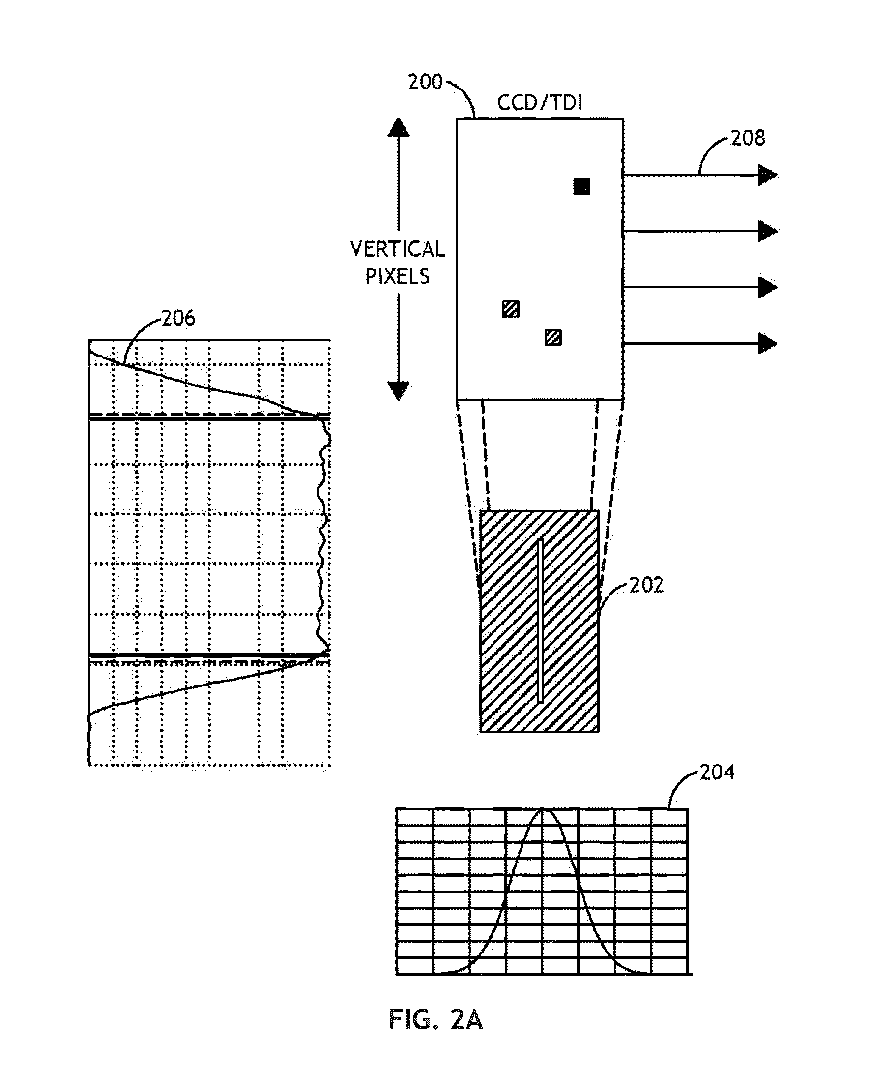
[0020]The process of time delay integration (TDI) and associated hardware are more fully described in U.S. Pat. No. 8,772,731; U.S. Pat. No. 8,624,971; U.S. Pat. No. 7,952,633; U.S. Pat. No. 7,609,309 and U.S. Pat. No. 7,227,984. Such processes and hardware are further described in U.S. Pat. App. Pub. No. 20140158864; U.S. Patent App. Pub. No. 20140043463; U.S. Patent App. Pub. No. 20130270444; U.S. Patent App. Pub. No. 20100188655; U.S. Patent App. Pub. No. 20060103725; U.S. Patent App. Pub. No. 20130016346 and U.S. Patent App. Pub. No. 2004...


PUM


Abstract

A wafer scanning system includes imaging collection optics to reduce the effective spot size. Smaller spot size decreases the number of photons scattered by the surface proportionally to the area of the spot. Air scatter is also reduced. TDI is used to produce a wafer image based on a plurality of image signals integrated over the direction of linear motion of the wafer. An illumination system floods the wafer with light, and the task of creating the spot is allocated to the imaging collection optics.

Description

FIELD OF THE INVENTION[0001]The present invention is directed generally toward inspection systems for semiconductor wafers and more particularly toward inspection systems with time delay integration (TDI) sensors.BACKGROUND OF THE INVENTION[0002]Time delay integration (TDI) is an imaging process that produces a continuous image of a moving two-dimensional object. In a TDI system, image photons are converted to photocharges in an array of pixels. As the object is moved, the photocharges are shifted from pixel to pixel down the sensor, parallel to the axis of movement. By synchronizing the photocharge shift rate with the velocity of the object, the TDI can integrate signal intensity at a fixed position on the moving object to generate the image. The total integration time can be regulated by changing the speed of the image motion and providing more / less pixels in the direction of the movement.[0003]TDI inspection systems can be used for inspecting wafers, masks, and / or reticles. A con...

Claims


Application Information

Patent Timeline
IPC IPC(8): G01N21/88G06T7/00G01N21/95
CPCG01N21/8851G01N21/9501G06T7/0004G01N2021/8887G06T2207/30148G01N2201/12G01N2201/06113G06T2207/10004G01N2201/103G01N21/956G01N2021/8896
Inventor VAZHAEPARAMBIL, JIJENZHAO, GUOHENGKAVALDJIEV, DANIELROMANOVSKY, ANATOLYMALEEV, IVANWOLTERS, CHRISTIANBIELLAK, STEPHENWHITESIDE, BRETPETTIBONE, DONALDCHUANG, YUNG-HO ALEXSHORTT, DAVID W.
Owner KLA TENCOR TECH CORP
Why Eureka
Try Eureka