Method of forming semiconductor device

a semiconductor and device technology, applied in the field of semiconductor device manufacturing, can solve the problems of generating undesired masking defects caused by polymer residues, oxide loss, and metal residues in dishing, and achieve the effect of improving device performan

Active Publication Date: 2016-04-07
UNITED MICROELECTRONICS CORP
View PDF0 Cites 0 Cited by
  • Summary
  • Abstract
  • Description
  • Claims
  • Application Information

AI Technical Summary

Benefits of technology

[0004]Accordingly, the present invention provides a method of forming a semiconductor structure, by which the conventional oxide loss and polymer residues are not observed so that the performance of the device can be effectively improved.

Problems solved by technology

However, during the step of removing the dummy gate, oxide loss (or called dishing) and polymer residues are usually observed on the surface of the dielectric layer.
In such case, metal residues remain in the dishing and undesired masking defects caused from the polymer residues are generated.
Therefore, the performance of the device is decreased.

Method used


Image

  • Method of forming semiconductor device
  • Method of forming semiconductor device
  • Method of forming semiconductor device

Examples


Embodiment Construction

[0029]Reference will now be made in detail to the present preferred embodiments of the invention, examples of which are illustrated in the accompanying drawings. Wherever possible, the same reference numbers are used in the drawings and the description to refer to the same or like parts.

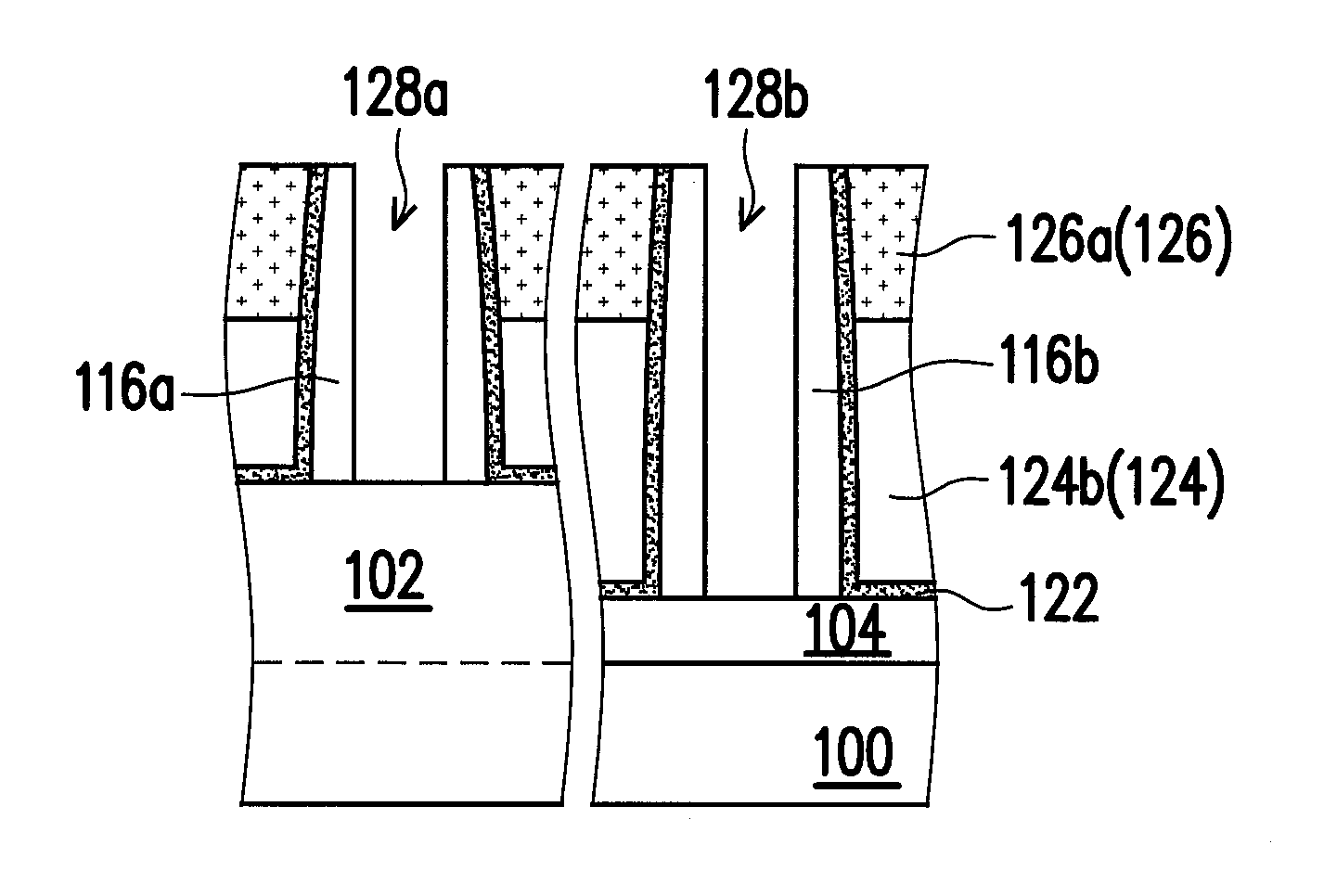
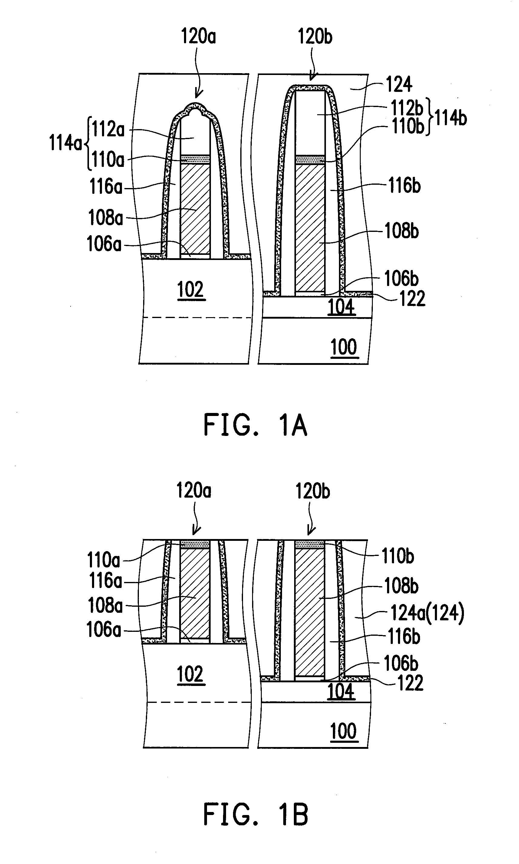
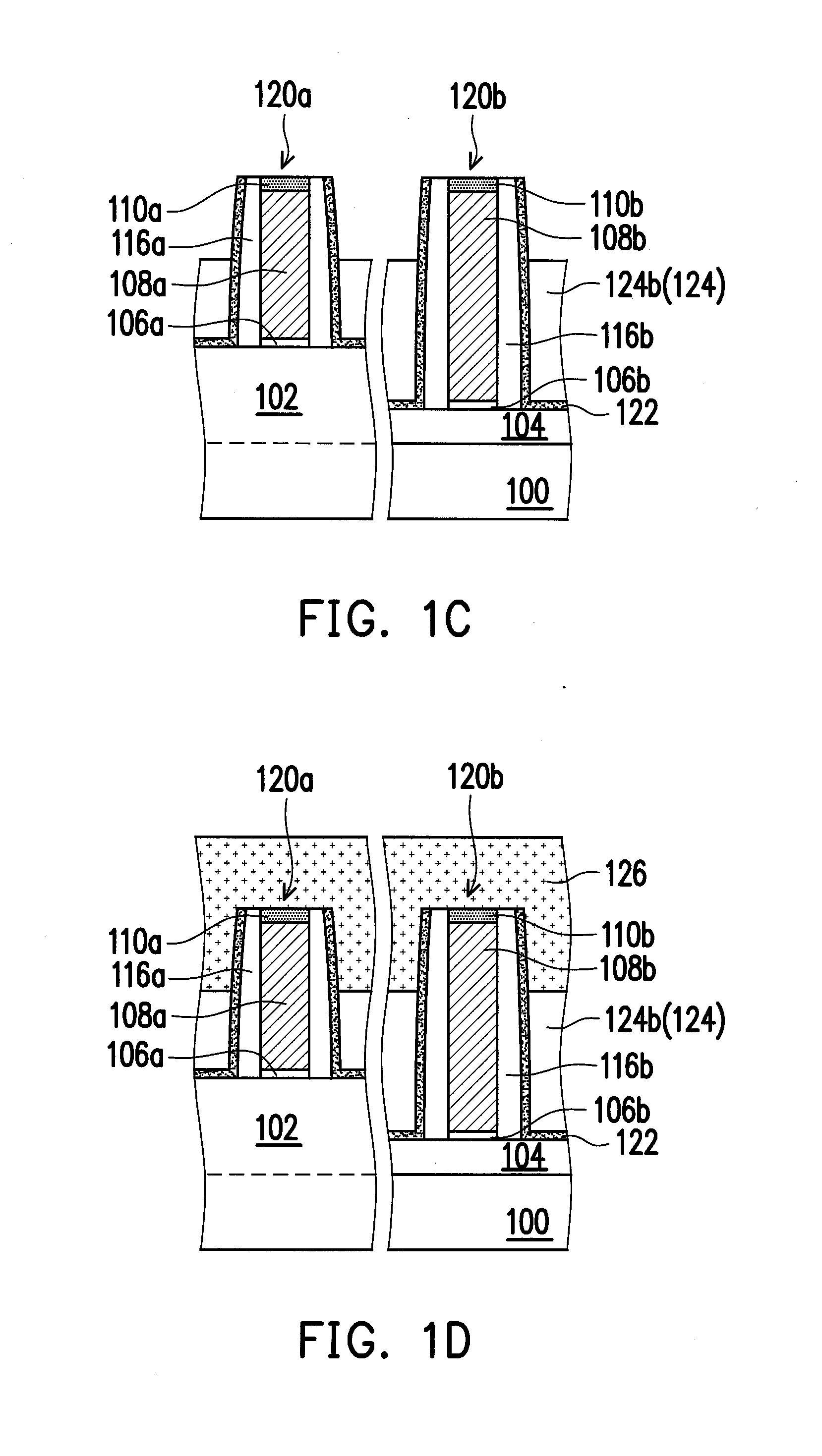
[0030]FIG. 1A to FIG. 1F are schematic cross-sectional views illustrating a method of forming a semiconductor device according to an embodiment of the present invention. In this embodiment, the method of the invention is integrated with a metal gate process for illustration.

[0031]Referring to FIG. 1A, a semiconductor substrate 100 is provided. The semiconductor substrate 100 can be a silicon-containing substrate with multiple fins 102 extending in a first direction. Thereafter, an insulating layer (or called a shallow trench isolation structure) 104 is formed to fill the lower portion of a gap between two adjacent fins 102. The insulating layers 104 include silicon oxide. The method of forming the in...


PUM


Abstract

A method of forming a semiconductor device is disclosed. A substrate having multiple fins is provided. An insulating layer fills a lower portion of a gap between two adjacent fins. At least one first stacked structure is formed on one fin and at least one second stacked structure is formed on one insulation layer. A first dielectric layer is formed to cover the first and second stacked structures. A portion of the first dielectric layer and portions of the first and second stacked structures are removed. Another portion of the first dielectric layer is removed until a top of the remaining first dielectric layer is lower than tops of the first and second stacked structures. A second dielectric layer is formed to cover the first and second stacked structures. A portion of the second dielectric layer is removed until the tops of the first and second stacked structures are exposed.

Description

FIELD OF THE PRESENT INVENTION[0001]The present invention relates to an integrated circuit (IC) fabrication, and particularly to a method of forming a semiconductor device.DESCRIPTION OF RELATED ART[0002]MOS is a basic structure widely applied to various semiconductor devices, such as memory devices, image sensors and display devices. An electric device is required to be made lighter, thinner and smaller. As the CMOS is continuously minimized, a logic CMOS technology is developed towards a technology having a high-k dielectric layer and a metal gate.[0003]The metal gate is usually formed by the following steps. First, a dummy gate is formed on a substrate, and then a dielectric layer is formed on the substrate outside of the dummy gate. Thereafter, the dummy gate is removed to form a gate trench, and then a metal gate is formed in the gate trench. However, during the step of removing the dummy gate, oxide loss (or called dishing) and polymer residues are usually observed on the surf...

Claims


Application Information

Patent Timeline
Patent Type & Authority Applications(United States)
IPC IPC(8): H01L21/8234H01L29/66H01L21/311H01L21/02H01L29/06H01L21/3105
CPCH01L21/823437H01L21/823431H01L29/0649H01L21/31055H01L29/66545H01L21/31144H01L21/0206H01L21/02271H01L21/311H01L21/02065H01L21/31053H01L21/823821H01L29/4966H01L29/517
Inventor LU, CHUN-TSENSU, CHIH-JUNGCHEN, JIAN-WEILU, SHUI-YENCHEN, YI-WENHUANG, PO-CHENGHUANG, CHEN-MINGTZOU, SHIH-FANG
Owner UNITED MICROELECTRONICS CORP
Why Eureka
Try Eureka