High Electron Mobility Transistor with Periodically Carbon Doped Gallium Nitride

Active Publication Date: 2016-04-07
KK TOSHIBA
View PDF8 Cites 9 Cited by
  • Summary
  • Abstract
  • Description
  • Claims
  • Application Information

AI Technical Summary

Benefits of technology

The patent describes a method of making a high electron mobility transistor (HEMT) device by growing a channel layer stack on a substrate, with alternating layers of undoped gallium nitride (GaN) and carbon doped GaN. A barrier layer is then formed on top of the channel layer stack, followed by the optional addition of a buffer layer. The method includes growing each layer with a specific ratio of group-V precursors to group-III precursors and a specific ratio of carbon concentration. The resulting HEMT device has improved performance and stability.

Problems solved by technology

For substrates other than bulk gallium nitride (GaN), it is difficult to epitaxially grow a high-quality gallium nitride (GaN) semiconductor crystal layer on substrate 102 due to poor lattice matching between the gallium nitride (GaN) and the substrate material.
However, the growth conditions that promote the incorporation of carbon (C) in gallium nitride (GaN) are in direct conflict with the growth conditions necessary to grow high-quality gallium nitride (GaN), which include high temperature, low growth rate, and a high ratio of group-V precursors to group-III precursors.
Because carbon doped gallium nitride (c-GaN) has inferior crystal quality and morphology, manufacturers are unable to grow the carbon doped gallium nitride (c-GaN) in thick layers, limiting the electrical breakdown performance of the HEMT device 100.
The structural defects present in carbon-doped gallium nitride (c-GaN) may also result in poor device performance and lower yield per wafer due to structural deterioration of the carbon-doped gallium nitride (c-GaN) material.
Moreover, a thick layer of carbon-doped gallium nitride (c-GaN) makes the HEMT device 100 unsuitable for an increasing number of end applications; particularly in light of the growing demand for smaller FET devices.

Method used


Image

  • High Electron Mobility Transistor with Periodically Carbon Doped Gallium Nitride
  • High Electron Mobility Transistor with Periodically Carbon Doped Gallium Nitride
  • High Electron Mobility Transistor with Periodically Carbon Doped Gallium Nitride

Examples


Embodiment Construction

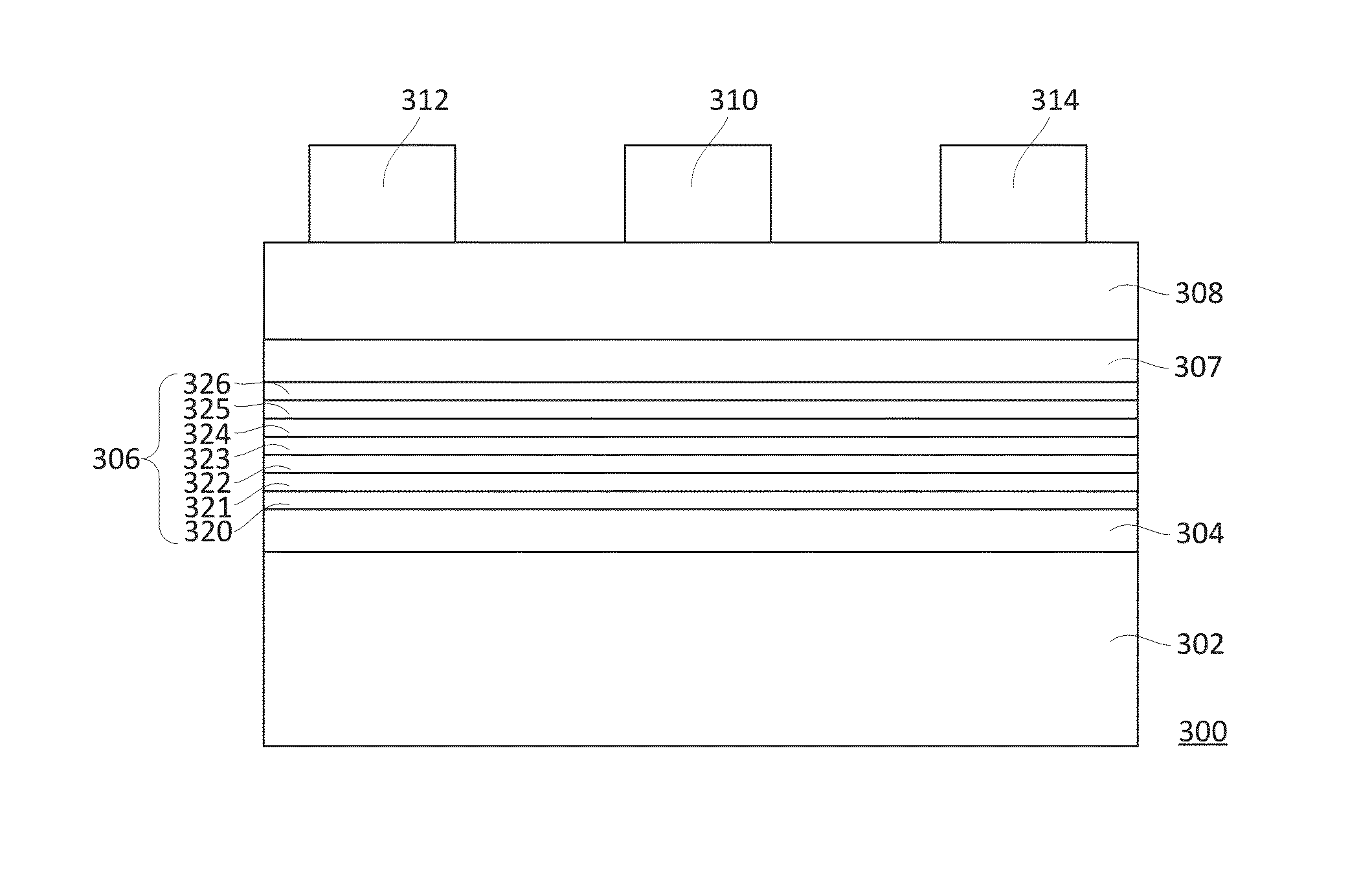
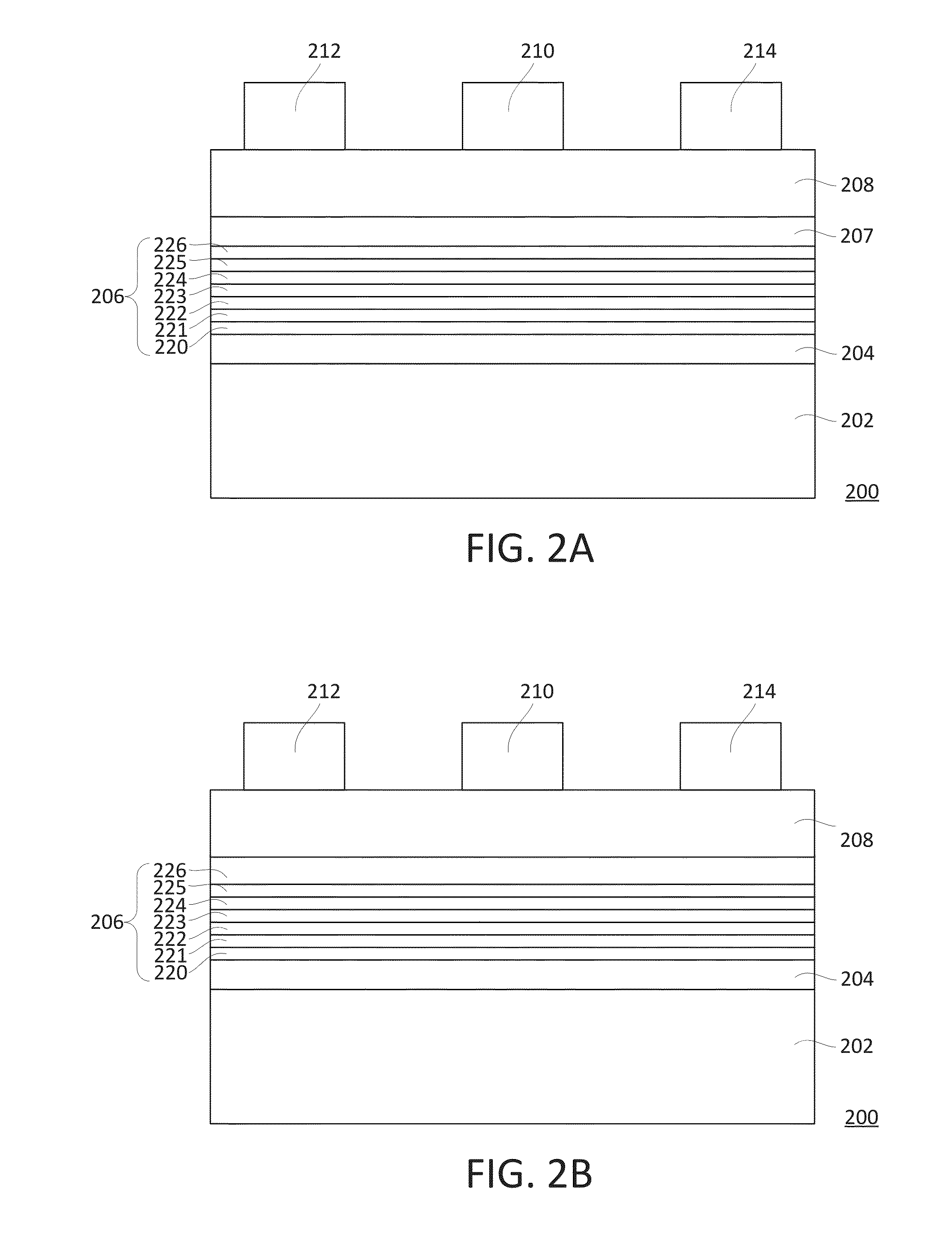
[0026]FIG. 2A shows a cross-sectional view of an HEMT device with alternating layers of undoped gallium nitride and carbon-doped gallium nitride, according to one embodiment of the invention. In FIG. 2, HEMT device 200 begins with substrate 202. Substrate 202 can be silicon (Si), silicon carbide (SiC), sapphire (Al2O3), bulk gallium nitride (GaN), or any other suitable substrate for epitaxially growing layers of gallium nitride (GaN). In one embodiment, not shown, the substrate 202 is bulk gallium nitride (GaN), and a plurality of alternating layers of undoped gallium nitride (GaN) and carbon doped gallium nitride (GaN) are epitaxially grown directly on top of the substrate 202.

[0027]In another embodiment, the substrate 202 is any suitable material for growing layers of gallium nitride (GaN), other than bulk gallium nitride (GaN). In this embodiment, a buffer layer 204 is deposited on top of substrate 202. Buffer layer 204 can be gallium nitride (GaN), aluminum gallium nitride (AlGa...


PUM


Abstract

A method for forming a high electron mobility transistor (HEMT) device with a plurality of alternating layers of one or more undoped gallium nitride (GaN) layers and one or more carbon doped gallium nitride layers (c-GaN), and an HEMT device formed by the method is disclosed. In one embodiment, the method includes forming a channel layer stack on a substrate, the channel layer stack having a plurality of alternating layers of one or more undoped gallium nitride (GaN) layers and one or more carbon doped gallium nitride layers (c-GaN). The method further includes forming a barrier layer on the channel layer stack. In one embodiment, the channel layer stack is formed by growing each of the one or more undoped gallium nitride (GaN) layers in growth conditions that suppress the incorporation of carbon in gallium nitride, and growing each of the one or more carbon doped gallium nitride (c-GaN) layers in growth conditions that promote the incorporation of carbon in gallium nitride.

Description

FIELD OF THE INVENTION[0001]The invention relates generally to high electron mobility transistors, and particularly to high electron mobility transistors with periodically carbon doped gallium nitride (GaN) layers.BACKGROUND OF THE INVENTION[0002]The high electron mobility transistor (HEMT) is a type of field effect transistor (FET) in which a hetero-junction between a channel layer and a barrier layer whose electron affinity is smaller than that of the channel layer is formed. A two-dimensional electron gas (2DEG) forms in the channel layer of a group III-V HEMT device due to the mismatch in polarization field at the channel-barrier layer interface. The 2DEG has a high electron mobility that facilitates high-speed switching during device operation. In typical HEMT devices, a negatively-biased voltage may be applied to the gate electrode to deplete the 2DEG and thereby turn off the device. A group III-V HEMT device is one made of materials in column III of the periodic table, such a...

Claims


Application Information

Patent Timeline
IPC IPC(8): H01L29/778H01L29/201H01L21/02H01L29/10H01L29/66H01L29/20H01L29/205
CPCH01L29/78H01L29/7787H01L29/2003H01L29/201H01L29/66H01L29/1029H01L29/66462H01L21/0254H01L21/02458H01L29/205H01L29/7785H01L29/7786H01L29/1075H01L29/207H01L21/02507H01L21/02579H01L21/0262
Inventor RAMER, JEFFREY CRAIGKNIERIEM, KARL
Owner KK TOSHIBA
Why Eureka
Try Eureka