Techniques for tiling arrays of pixel elements and fabricating hybridized tiles

a technology of hybridization and arrays, applied in the field of fabrication and assembly of tiles, can solve the problems of inevitability of damage to the edge of sub-array tiles (chips), and achieve the effect of reducing complexity

Inactive Publication Date: 2016-04-14
SANTA BARBARA INFRARED
View PDF3 Cites 17 Cited by
  • Summary
  • Abstract
  • Description
  • Claims
  • Application Information

AI Technical Summary

Benefits of technology

[0023]It is an object of the invention(s) to provide improved techniques for tiling sub-arrays of pixel elements to implement larger arrays, such as megapixel arrays. For example, the techniques disclosed herein address avoiding or circumventing problems associated with the seams between tiles which may include (i) artifacts of the seams manifesting themselves in the projected image, and (ii) damage to edge pixels in the sub-arrays (tiles, chips) due to manufacturing processes. Additionally, the techniques disclosed herein may eliminate the complexity associated with some prior art techniques of overcoming the seam problem.

Problems solved by technology

Some damage to the edge of a sub-array tile (chip) is inevitable (unavoidable) as a result of manufacturing process (cutting, dicing, etc.).

Method used


Image

  • Techniques for tiling arrays of pixel elements and fabricating hybridized tiles
  • Techniques for tiling arrays of pixel elements and fabricating hybridized tiles
  • Techniques for tiling arrays of pixel elements and fabricating hybridized tiles

Examples


Embodiment Construction

[0056]Various embodiments will be described to illustrate teachings of the invention(s), and should be construed as illustrative rather than limiting. Any dimensions and materials or processes set forth herein should be considered to be approximate and exemplary, unless otherwise indicated.

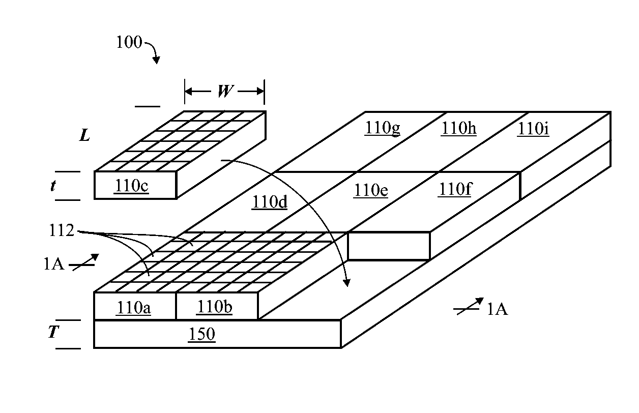
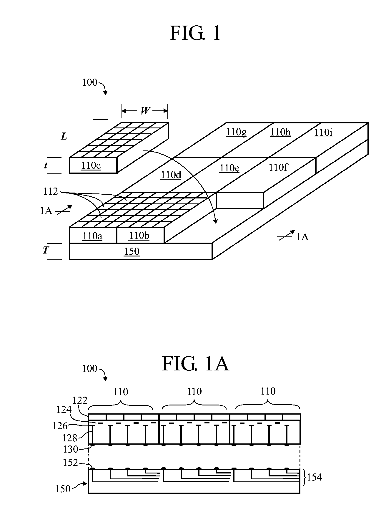
[0057]The present disclosure is directed to techniques for fabricating large arrays of pixels from tiling smaller arrays (sub-arrays or tiles), where there is a sub-pixel (less than the pitch of a pixel) to zero gap at the seams between tiles. The basic concept is to route all I / O (power and data) through the back of the array so that the tiles can be placed edge-to-edge on all sides. The small arrays can then be arranged into a larger M×N array. This technique is applicable to both imaging systems as well as to projection systems.

[0058]In general, infrared (IR) radiation may have a range of wavelengths of 0.8-20 μm or larger though the most common wavelengths uses for thermal imagery are 3-5 um (...


PUM

PropertyMeasurementUnit
wavelengthsaaaaaaaaaa

Abstract

A first substrate having an array of emitters or detectors may be joined by bump bonding with a second substrate having read-in (RIIC) or read-out (ROIC) circuitry. After the two substrates are joined, the resulting assembly may be singulated to form sub-arrays such as tiles sub-arrays having pixel elements which may be arranged on a routing layer or carrier to form a larger array. Edge features of the tiles may provide for physical alignment, mechanical attachment and chip-to-chip communication. The pixel elements may be thermal emitter elements for IR image projectors, thermal detector elements for microbolometers, LED-based emitters, or quantum photon detectors such as those found in visible, infrared and ultraviolet FPAs (focal plane arrays), and the like.

Description

CROSS-REFERENCE TO RELATED APPLICATION(S)[0001]This is a continuation-in-part of Ser. No. 13 / 656,711 filed 21 Oct. 2012 (U.S. Pat. No. 9,163,995 20 Oct. 2015) by Laveigne et al., which claims priority from U.S. 61 / 550,350 filed Oct. 21, 2011.TECHNICAL FIELD[0002]The invention relates to fabricating and assembling tiles (chips, sub-arrays) of pixel elements into larger arrays, more particularly pixel elements which may be thermal radiation emitters such as resistive pixel elements for infrared (IR) image projection, thermal radiation detectors such as for a microbolometer, and the like.BACKGROUND[0003]The human eye cannot detect infrared light. But infrared energy can be detected electronically. Sophisticated electronic instruments exist which can scan a scene and convert the infrared light to an electrical signal which can be displayed on a video monitor, analyzed by a computer, or recorded on film. Electrically, the output of these instruments is very similar to the output of a con...

Claims


Application Information

Patent Timeline
Patent Type & Authority Applications(United States)
IPC IPC(8): H01L25/16H01L33/62H01L31/18H01L33/00G01J1/44H01L27/146
CPCH01L25/167G01J1/44H01L27/14634H01L27/14636H01L2933/0066H01L27/1469H01L31/186H01L33/0095H01L33/62H01L27/14649G01J5/20Y10T29/49002Y10T29/49117H01L2924/0002G01J5/045G01J5/024G01J2005/106G01J2005/202H01L2924/00G01J5/02
Inventor LAVEIGNE, JOSEPH DONALD
Owner SANTA BARBARA INFRARED
Why Eureka
Try Eureka