Methods for producing low oxygen silicon ingots

a technology of silicon ingots and oxygen concentration, which is applied in the direction of polycrystalline material growth, crystal growth process, polycrystalline material growth, etc., can solve the problems of reducing the yield of semiconductor devices fabricated using ingots, wafers may have relatively weak mechanical strength, and relatively poor slip performan

Active Publication Date: 2016-04-21
GLOBALWAFERS CO LTD
View PDF0 Cites 26 Cited by
  • Summary
  • Abstract
  • Description
  • Claims
  • Application Information

AI Technical Summary

Problems solved by technology

The oxygen may cause various defects in wafers produced from the ingots, reducing the yield of semiconductor devices fabricated using the ingots.
Due to the relatively low Oi, such wafers may have relatively weak mechanical strength and relatively poor slip performance at high temperature anneal / ramp that may be requested by a device manufacturer.
However, float zone materials are relatively expensive and are limited to use in producing ingots having a diameter less than about 200 mm.
Accordingly, these known methods are unable to produce higher diameter silicon crystal ingots with a relatively low oxygen concentration.

Method used


Image

  • Methods for producing low oxygen silicon ingots
  • Methods for producing low oxygen silicon ingots
  • Methods for producing low oxygen silicon ingots

Examples


Embodiment Construction

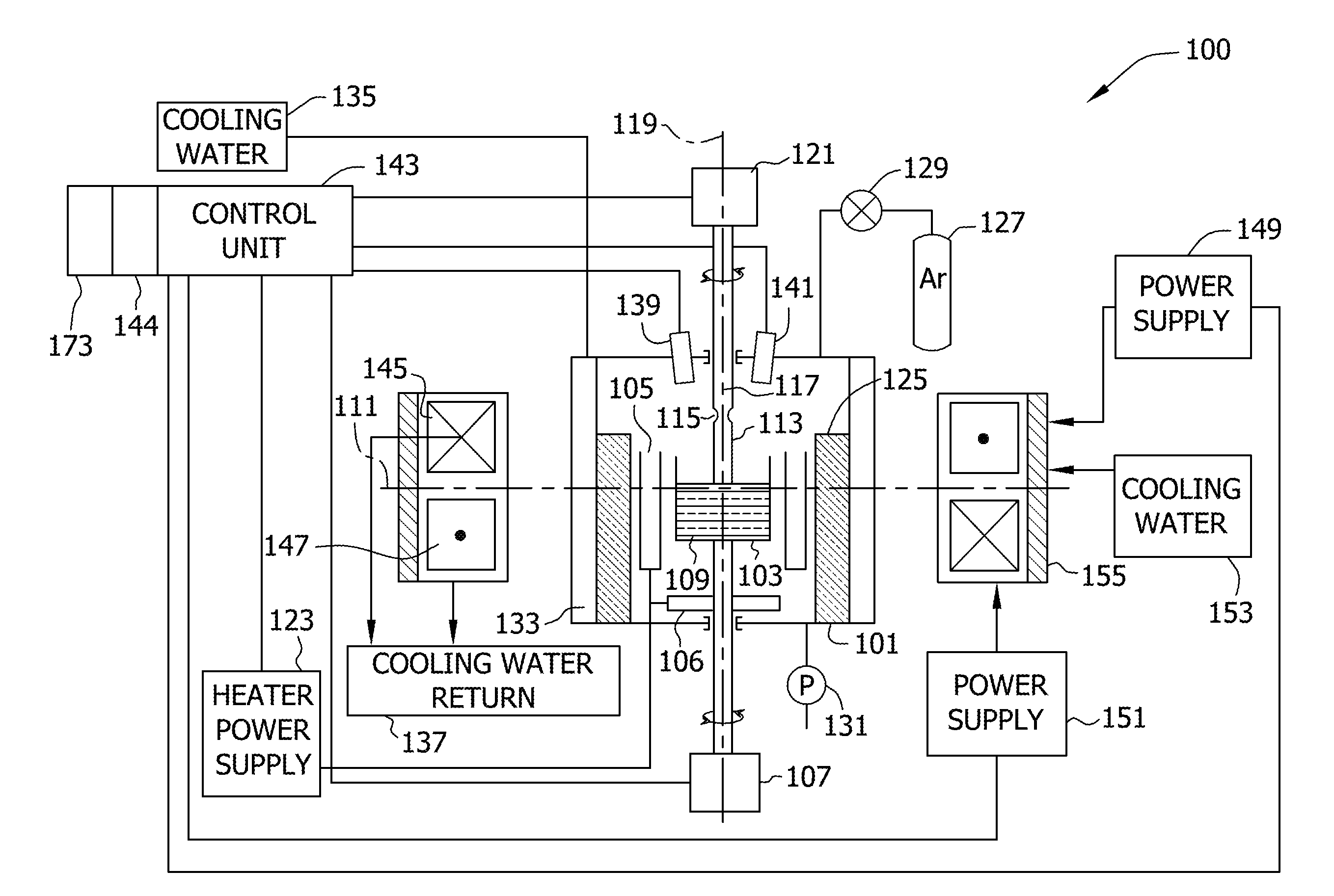
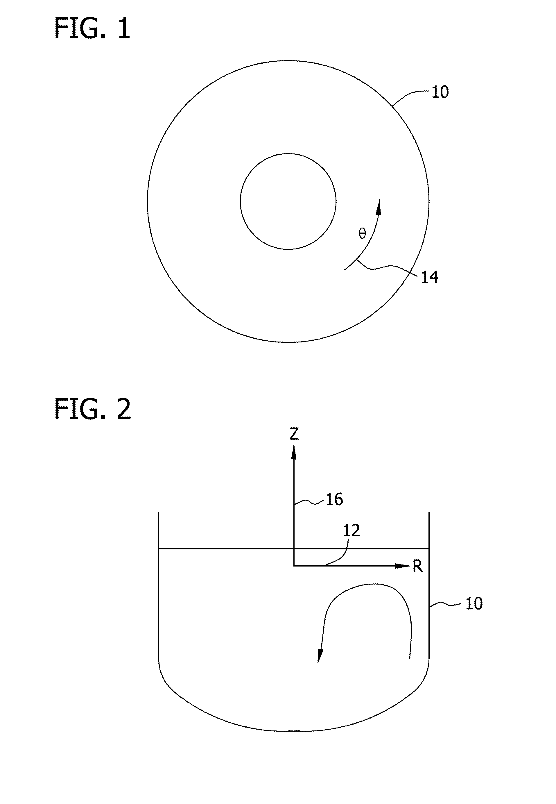
[0025]Referring initially to FIGS. 1 and 2, a crucible of one embodiment is indicated generally at 10. A cylindrical coordinate system for crucible 10 includes a radial direction R 12, an angular direction θ14, and an axial direction Z 16. Coordinates R 12, θ14, and Z 16 are used herein to describe methods and systems for producing low oxygen silicon ingots.

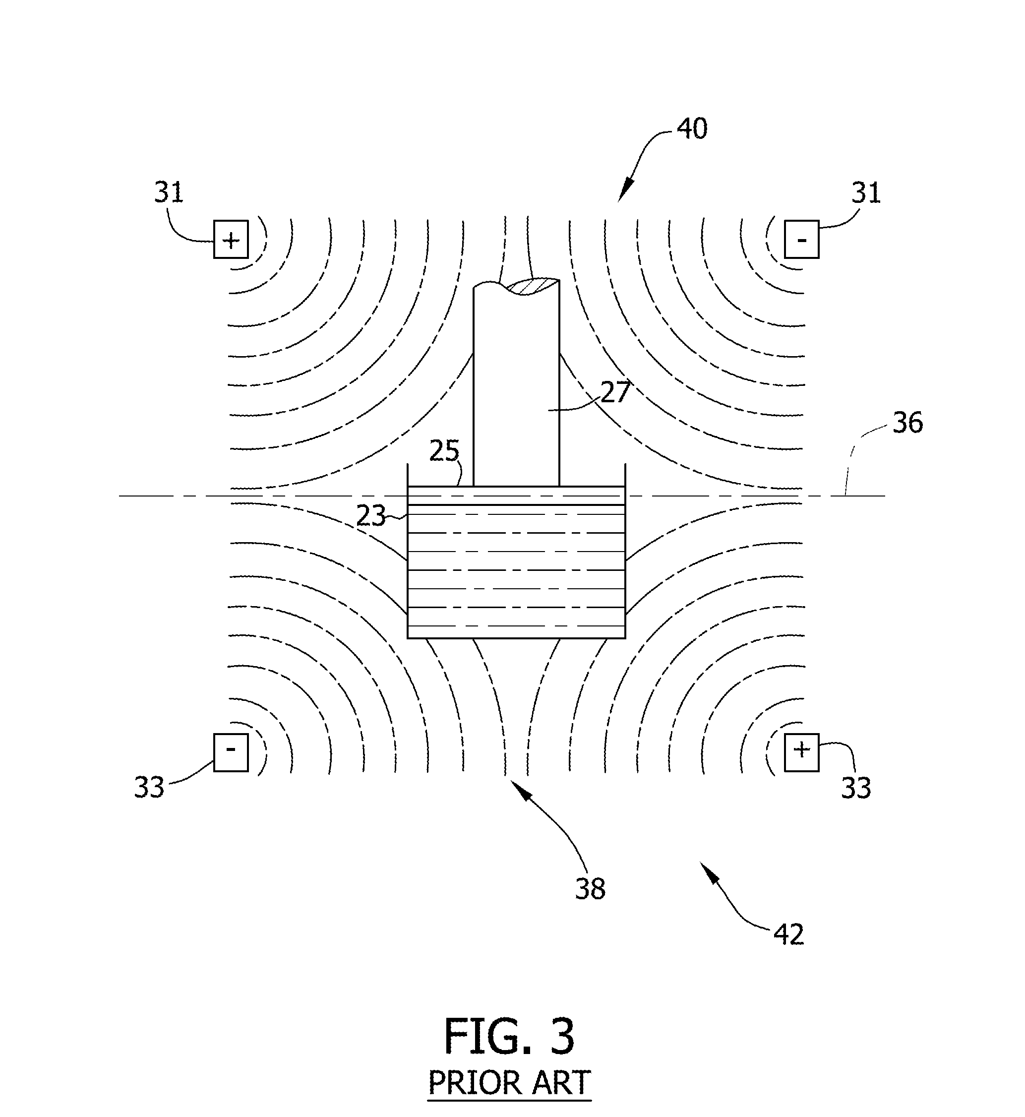
[0026]FIG. 3 is a block diagram illustrating a cusped magnetic field being applied to a crucible 23 containing a melt 25 in a crystal growing apparatus. As shown, crucible 23 contains silicon melt 25 from which a crystal 27 is grown. The cusped magnetic field configuration is designed to overcome deficiencies of axial and horizontal magnetic field configurations. A pair of coils 31 and 33 (e.g., Helmholtz coils) are placed coaxially above and below a melt surface 36. Coils 31 and 33 are operated in an opposed current mode to generate a magnetic field that has a purely radial field component (i.e., along R 12) near melt surface 36...


PUM

PropertyMeasurementUnit
diameteraaaaaaaaaa
diameteraaaaaaaaaa
diameteraaaaaaaaaa

Abstract

An method for producing a silicon ingot includes melting polycrystalline silicon in a crucible enclosed in a vacuum chamber to form a melt, generating a cusped magnetic field within the vacuum chamber, dipping a seed crystal into the melt, withdrawing the seed crystal from the melt to pull a single crystal that forms the silicon ingot, wherein the silicon ingot has a diameter greater than about 150 millimeters (mm), and simultaneously regulating a plurality of process parameters such that the silicon ingot has an oxygen concentration less than about 5 parts per million atoms (ppma). The plurality of process parameters include a wall temperature of the crucible, a transport of silicon monoxide (SiO) from the crucible to the single crystal, and an evaporation rate of SiO from the melt.

Description

CROSS-REFERENCE TO RELATED APPLICATION[0001]This application claims priority to U.S. Provisional Patent Application No. 61 / 827,393 filed on May 24, 2013, the entire disclosure of which is hereby incorporated by reference in its entirety.FIELD[0002]This disclosure generally relates to silicon ingots, and more specifically, to producing silicon ingots having a low oxygen concentration.BACKGROUND[0003]Single crystal silicon is the starting material in many processes for fabricating semiconductor electronic components and solar materials. For example, semiconductor wafers produced from silicon ingots are commonly used in the production of integrated circuit chips on which circuitry is printed. In the solar industry, single crystal silicon may be used instead of multicrystalline silicon due to the absence of grain boundaries and dislocations.[0004]To produce the semiconductor or solar wafers, a single crystal silicon ingot may be produced by melting polycrystalline silicon in a crucible ...

Claims


Application Information

Patent Timeline
Patent Type & Authority Applications(United States)
IPC IPC(8): C30B15/20C30B15/30H01L29/165C30B30/04H01L29/739H01L29/167C30B15/04C30B29/06
CPCC30B15/20C30B15/04C30B15/30H01L29/165C30B30/04H01L29/7393H01L29/167C30B29/06C30B15/305
Inventor BASAK, SOUBIRHUDSON, CARISSIMA MARIESAMANTA, GAURABRYU, JAE-WOOSREEDHARAMURTHY, HARIPRASADMCCALLUM, KIRK D.LEE, HYUNGMIN
Owner GLOBALWAFERS CO LTD
Why Eureka
Try Eureka