Modular interdigitated back contact photovoltaic cell structure on opaque substrate and fabrication process

a photovoltaic cell and module technology, applied in photovoltaic energy generation, electrical equipment, climate sustainability, etc., can solve the problem of less diffused short circuits, achieve efficient and low cost, large size, and simple and low cost

Inactive Publication Date: 2016-04-21
STMICROELECTRONICS SRL
View PDF4 Cites 6 Cited by
  • Summary
  • Abstract
  • Description
  • Claims
  • Application Information

AI Technical Summary

Benefits of technology

[0012]An efficient back contacted solar cell structure and an effective process of fabrication that lends itself to the formation of interconnected arrays of cells according to a desired series-parallel scheme, directly over substrates of relatively large dimension, using simple and low cost techniques industrially usable for producing efficient and low cost panels of large sizes, are herein disclosed.
[0017]The spacing / isolating stripes of undoped polysilicon between adjacent p+ and n+ doped regions effectively isolate laterally adjacent active regions of opposite type of conductivity, minimizing efficiency losses in the process of conversion of the photonic energy in the blanket layer of semiconducting polysilicon that acts as intrinsic semiconductor of the integrated structure of the photodiode. The photodiode may be of multijunction type and, for some peculiarities, similar to a pin or nip structure, equating the absorption layer to the intrinsic semiconductor region i or the pin or nip diodes of photovoltaic cells of amorphous silicon.
[0023]The interdigitated back contacted integrated photodiode cell structure may be economically and easily fabricable even on large size substrates for realizing arrays of a theoretically unlimited number of cells, the electrical terminations of which may be pre-ordinately interconnected according to a certain series-parallel scheme over the surface of the substrate. The geometrical details of the integrated structure are definable with techniques applicable to substrates of large size, such as of deposition, heat treatment, laser scribing steps, printing and lithography.

Problems solved by technology

However, the laser scribing technique of localized fusion may augment crystal lattice defectivity which, though localized, may sensibly penalize conversion efficiency, by causing more or less diffused short circuits among distinct electrical structures of the integrated photodiode.

Method used


Image

  • Modular interdigitated back contact photovoltaic cell structure on opaque substrate and fabrication process
  • Modular interdigitated back contact photovoltaic cell structure on opaque substrate and fabrication process
  • Modular interdigitated back contact photovoltaic cell structure on opaque substrate and fabrication process

Examples


Embodiment Construction

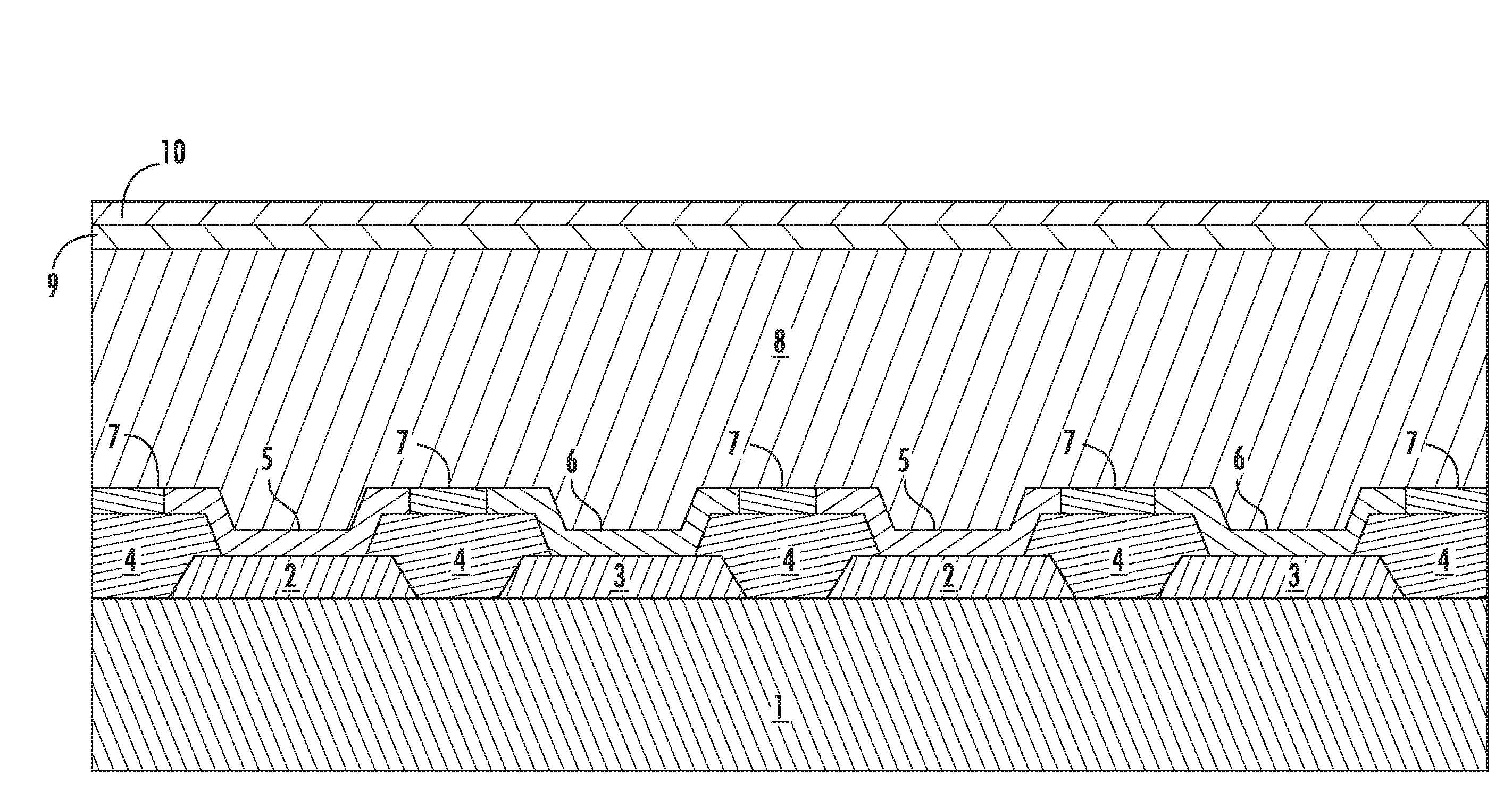
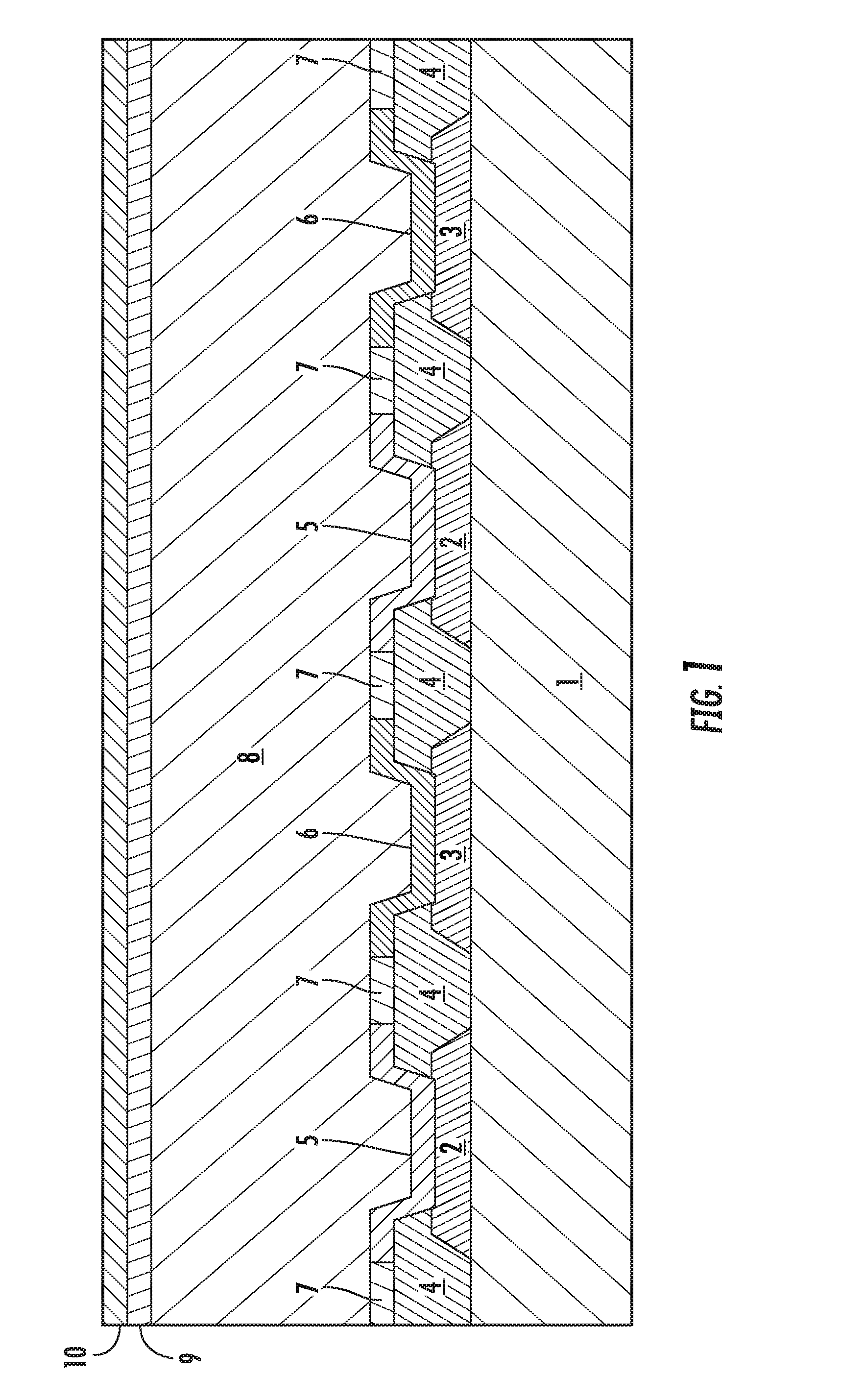
[0030]An exemplary embodiment of the novel integrated structure of a polycrystalline silicon diode, or of least partially crystalline silicon at of the photovoltaic cell, of this disclosure is shown in the partial cross sectional view of FIG. 1.

[0031]The mechanical supporting substrate 1 may be of any metallic, ceramic or glass-ceramic material suitable to withstand process temperatures, of values ranging from about 600 to about 1,000° C., and possibly up to about 1,200° C., or even higher.

[0032]Examples of suitable materials are titanium, the surface of which may be rendered electrically insulating by growing a surface oxide film, anodized aluminum (suitably limiting the maximum process temperature), sheet copper, nickel, stainless steel or hastelloy provided with a ceramic coat, ceramic or glass-ceramic plates.

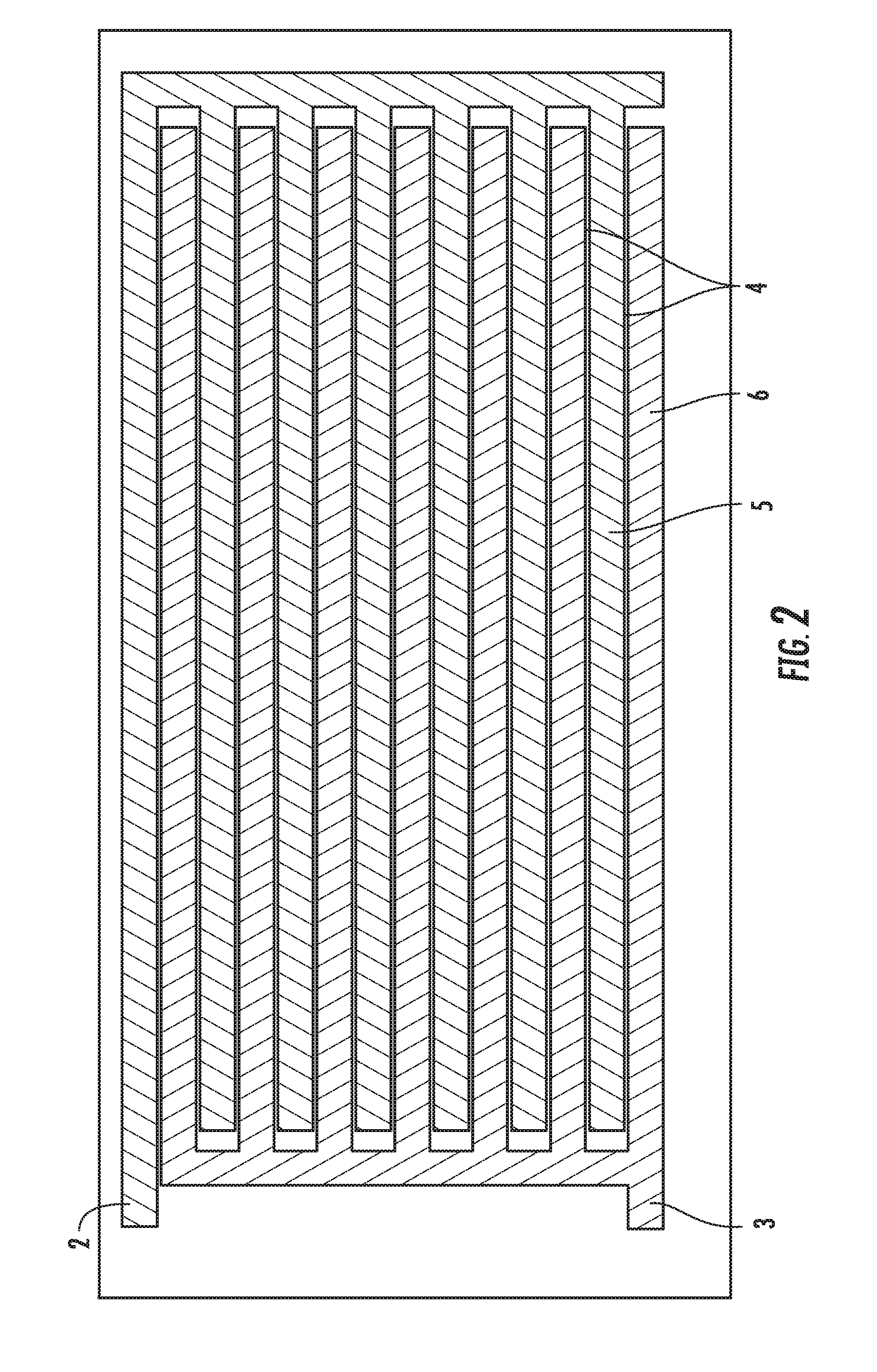
[0033]Two distinct interdigitated electrode structures 2 and 3 of back contact and electrical connection of the cell may be made of the same metallic material, and may be ad...


PUM


Abstract

A back contact integrated photovoltaic cell includes a substrate having a dielectric surface and a patterned metal layer with parallel spaced alternately positive and negative electrode fingers forming an interdigitated two-terminal structure over the dielectric surface of the substrate. A dielectric filler may be in the interstices of separation between adjacent spaced parts of the patterned metal layer. Parallel spaced strips, alternately of p+ doped polysilicon and of n+ doped polysilicon, may top the positive and negative interdigitated electrode fingers, respectively, and form doped p-type active regions and n-type active regions of the integrated photovoltaic cell, spaced and isolated by a strip of undoped or negligibly doped polysilicon. An n− or p− doped or intrinsic semiconducting layer of at least partly crystallized silicon, forming a semiconductor region of thickness adapted to maximize absorption of photonic energy when illuminated by sunlight, may cover the interdigitated active doped regions.

Description

FIELD OF THE INVENTION[0001]The present disclosure relates, in general, to thin film photovoltaic cells for converting solar radiation (solar cells) formed at the surface of a substrate and, in particular, to back contacted vertical cells and related fabrication processes.BACKGROUND OF THE INVENTION[0002]Solar cells are conversion devices of solar radiation to electrical energy. In general, the cells are made by forming P-type regions and N-type regions in a semiconductor material (photodiodes). The solar radiation, by illuminating the cell, generates electron / vacancy pairs that migrate respectively towards the P-type region and the N-type region, creating a voltage difference at the diode terminals.[0003]In a back contacted solar cell, both N-type doped and P-type doped regions, commonly interdigitated between each other, as well as the current collecting electrodes respectively connected to them that may also form the connecting terminals of a cell to an electric load using the ge...

Claims


Application Information

Patent Timeline
Patent Type & Authority Applications(United States)
IPC IPC(8): H01L31/18H01L31/068H01L31/0224
CPCH01L31/182H01L31/0682H01L31/022441H01L31/046Y02E10/546Y02P70/50H01L31/1872Y02E10/547
Inventor CAMALLERI, CATENO MARCOLORENTI, SIMONAMANGANO, FABRIZIO
Owner STMICROELECTRONICS SRL
Why Eureka
Try Eureka