

Epoxy resin composition for optical semiconductor device, and lead frame for optical semiconductor device, encapsulation type optical semiconductor element unit and optical semiconductor device each obtainable by using the epoxy resin composition
a technology of epoxy resin and semiconductor, which is applied in the direction of semiconductor/solid-state device details, camera filters, instruments, etc., can solve the problems of reducing workability and difficult to ensure both fluidity and workability in the molding step, and achieves excellent blocking resistance, suppressing warpage, and free from moldability reduction
- Summary
- Abstract
- Description
- Claims
- Application Information
AI Technical Summary
Benefits of technology
Problems solved by technology
Method used
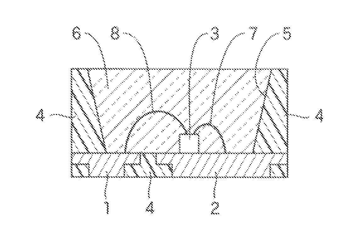
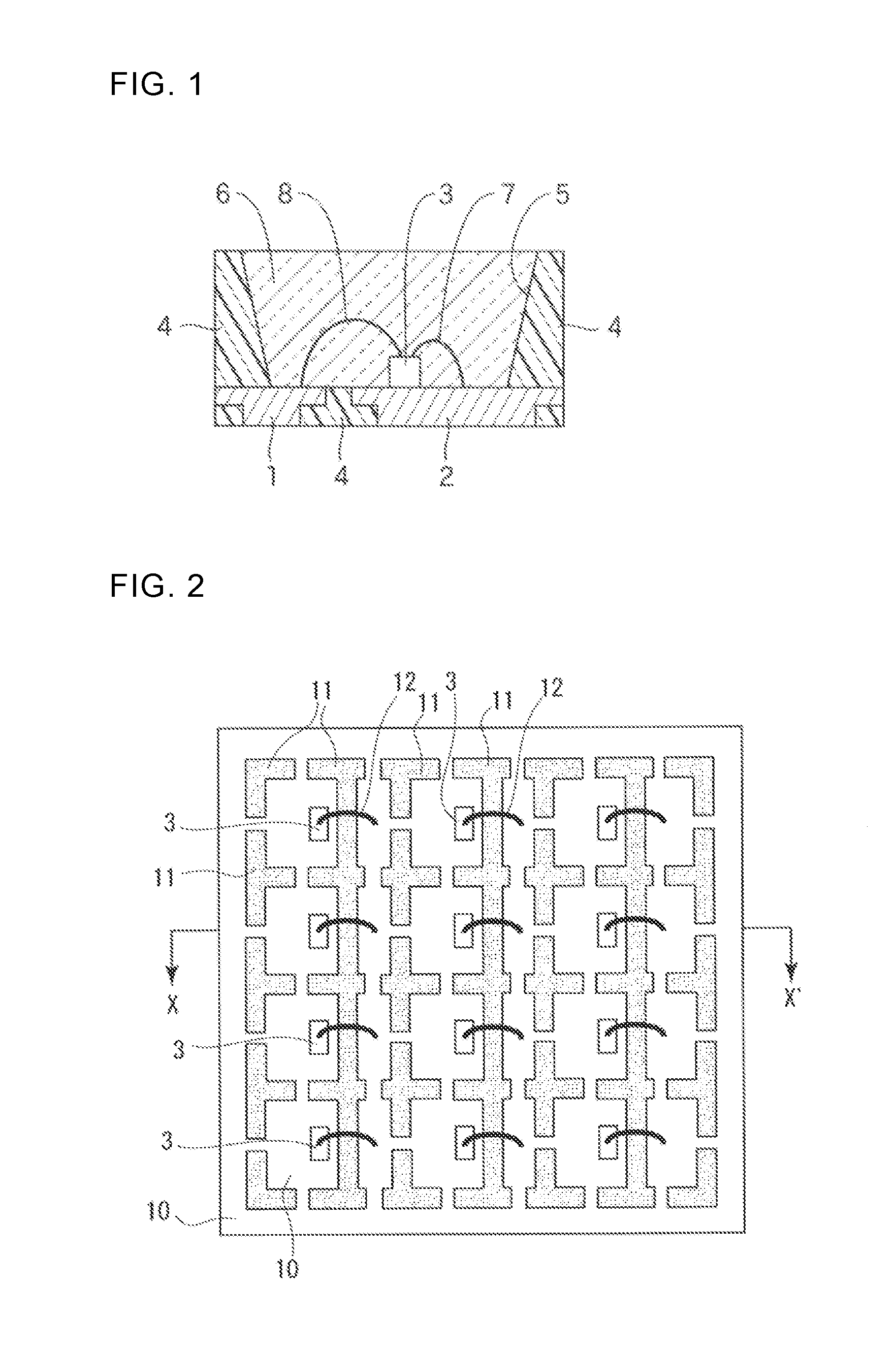
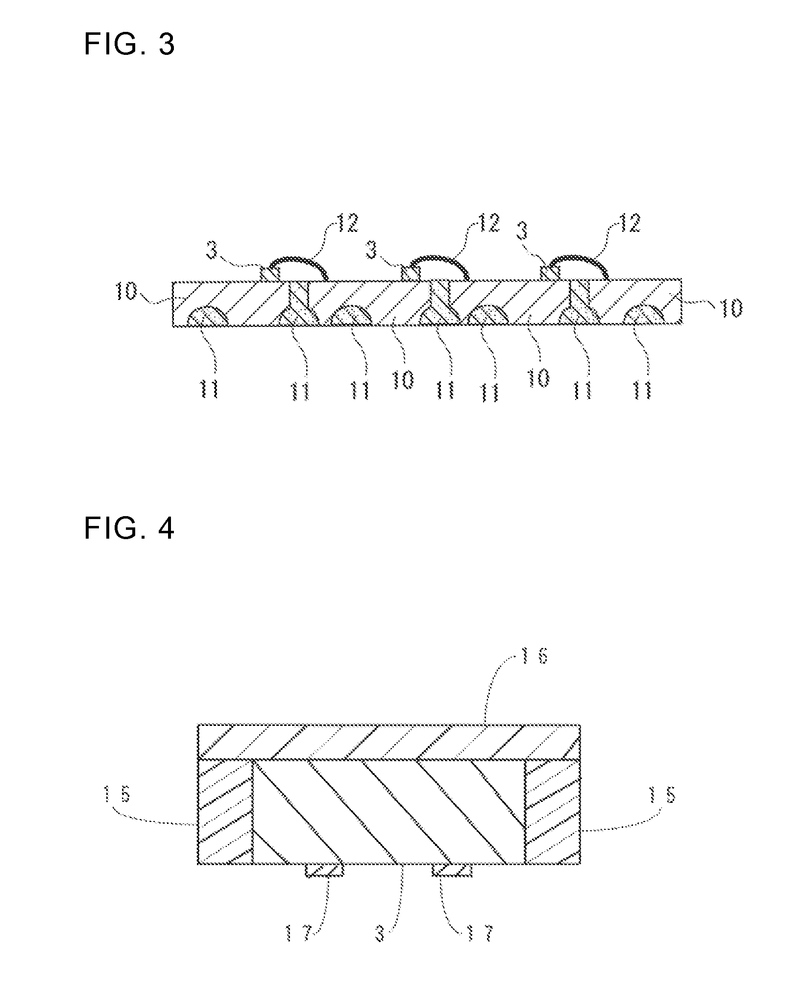
Image

Examples
examples
[0070]Inventive examples will hereinafter be described in conjunction with comparative examples. However, it should be understood that the invention be not limited to these inventive examples.
[0071]The following ingredients were prepared before preparation of epoxy resin compositions.
[0072][Epoxy Resin]
[0073]Tris(2,3-epoxypropyl)isocyanurate (TEPIC-S available from Nissan Chemical Industries, Ltd.)
[0074][Curing Agent]
[0075]A mixture containing 4-methylhexahydrophthalic anhydride (x) and hexahydrophthalic anhydride (y) in a mixing weight ratio of x:y=70:30 (RIKACID MH-700 available from New Japan Chemical Co., Ltd.)
[0076][Carboxylic Acid]
[0077]Hexahydrophthalic acid (RIKACID HH-W in solid form treated so as to have an average particle diameter of not greater than 500 μm, and available from New Japan Chemical Co., Ltd.)
[Water]
[0078]Deionized Water
[0079][Plasticizer f1]
[0080]Neopentyl glycol (available from Mitsubishi Gas Chemical Company, Inc.)
[0081][Plasticizer f2]
[0082]Trimethylolpr...
PUM
| Property | Measurement | Unit |
|---|---|---|
| softening point | aaaaa | aaaaa |
| particle diameter | aaaaa | aaaaa |
| particle diameter | aaaaa | aaaaa |
Abstract
Description
Claims
Application Information