Multi-layer printed circuit boards suitable for layer reduction design

Active Publication Date: 2016-04-28
ELITE MATERIAL
View PDF0 Cites 5 Cited by
  • Summary
  • Abstract
  • Description
  • Claims
  • Application Information

AI Technical Summary

Benefits of technology

[0012]By using the glass fiber cloth and insulation layers with specified dielectric constant, the present invention is capable of

Problems solved by technology

In addition, it is well-known that circuit board production involves many different processes, at least including cutting, baking, mechanical drilling (alignment holes), fabrication of inner circuits, layer build-up lamination, laser drilling, exposure and development, fabrication of inner circuits, layer build-up lamination, laser drilling, exposure and development, fabrication of inner circuits and so on, and the formation of each additional circuit layer requires the repetition of

Method used


Image

  • Multi-layer printed circuit boards suitable for layer reduction design
  • Multi-layer printed circuit boards suitable for layer reduction design
  • Multi-layer printed circuit boards suitable for layer reduction design

Examples


embodiments

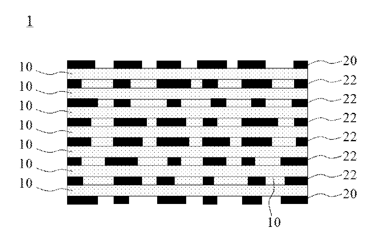
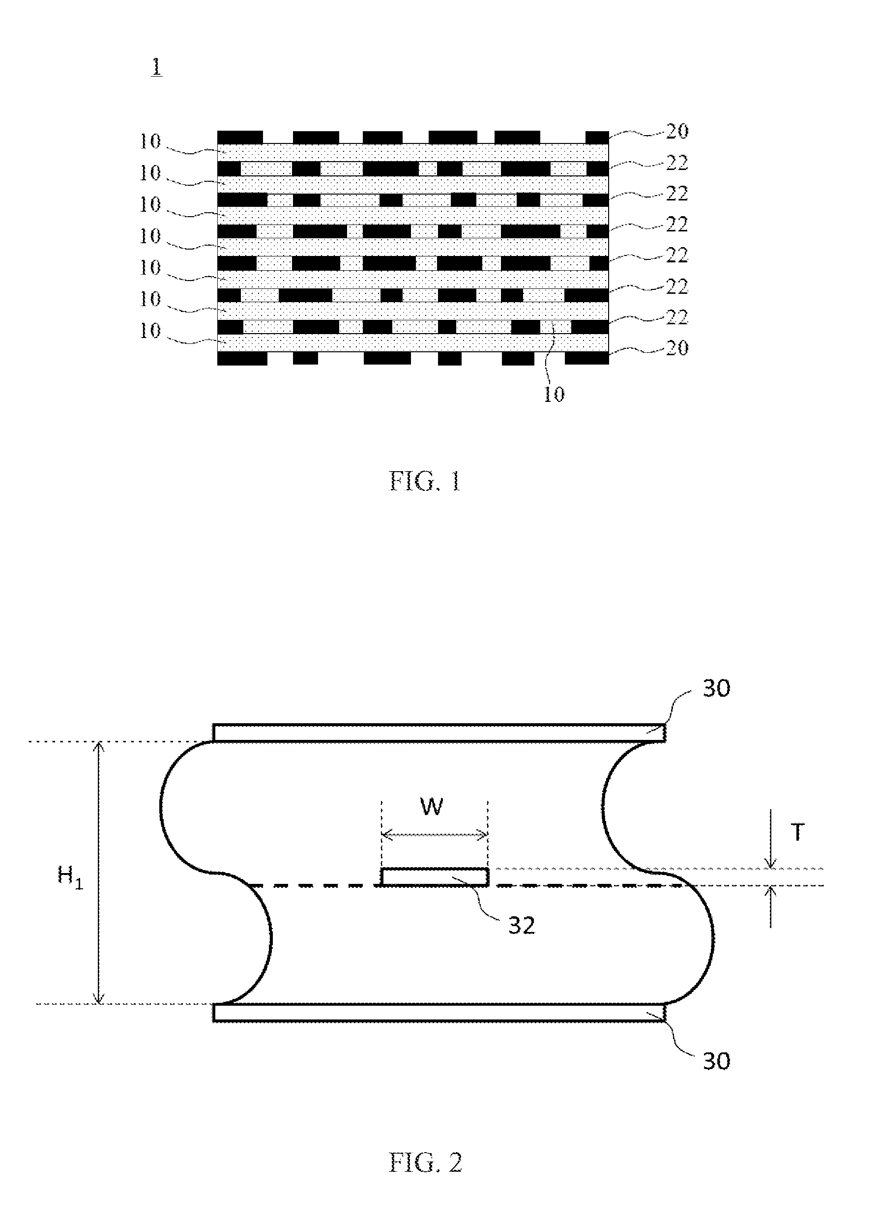
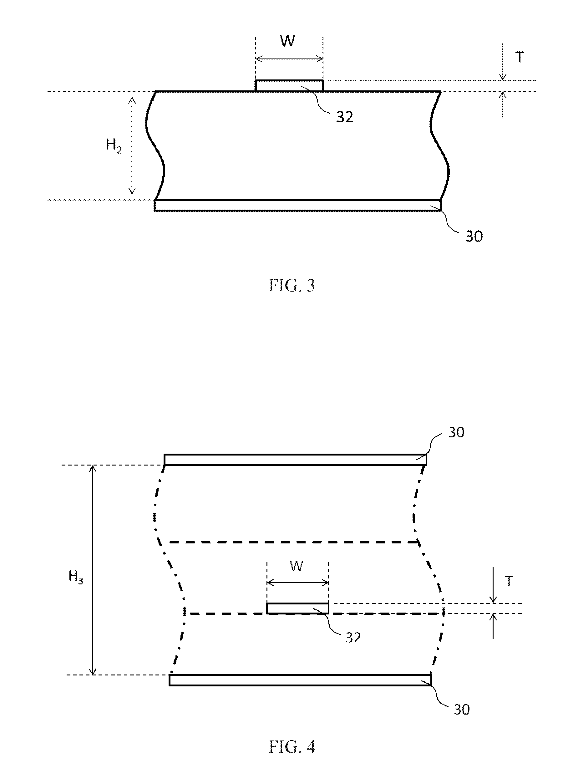
[0039]For clarity and completeness, E1 through E7 below represent different examples of circuit boards according to the present disclosure, and C1 through C5 below represent different comparative examples of circuit boards according to the present disclosure. In Example 1 (E1), EM-355(D) prepregs (E-glass fabric, type 1037, resin content 75%) sold by Elite Material Co., Ltd. are used to make an eight-layer circuit board following the processes of conventional layer reduction techniques. In Example 2 (E2), EM-355(D)K prepregs (L-glass fabric, type 1037, resin content 75%) sold by Elite Material Co., Ltd. are used to make an eight-layer circuit board following the processes of conventional layer reduction techniques. In Examples 3 to 7 (E3 to E7), various ingredients of resin composition A3 shown in Table 1 are well mixed to prepare resin varnish, and L-glass fabric (1037) or NE-glass fabric is impregnated with the varnish to prepare a prepreg (resin content 75%); then a plurality of ...


PUM

PropertyMeasurementUnit
Lengthaaaaaaaaaa
Lengthaaaaaaaaaa
Fractionaaaaaaaaaa

Abstract

A multi-layer printed circuit board comprises: at least two insulation layers, respectively having glass fiber cloth and cured resin covering thereon, the insulation layers being stacked on each other; an internal trace layer formed between two neighboring insulation layers; and an external trace layer formed on an outer surface of the outermost insulation layer; wherein the insulation layers have a dielectric constant of 3.4 or less, and the internal and external trace layers have a trace width between 40 and 75 micrometers, such that the multi-layer printed circuit board has a characteristic impedance between 45 and 55 Ω in single-ended signaling and between 90 and 110 Ω in differential signaling.

Description

CROSS-REFERENCE TO RELATED APPLICATIONS[0001]This application claims priority of Taiwan Patent Application No. 103136553, filed on Oct. 23, 2014, the entirety of which is incorporated by reference herein.FIELD OF THE INVENTION[0002]The present invention relates to multi-layer printed circuit boards suitable for layer reduction design and more particularly to multi-layer printed circuit boards with better transmission property and higher process yield rate after multiple laminations where thickness reduction or layer reduction is implemented.BACKGROUND OF THE INVENTION[0003]Printed circuit boards (PCBs) are critical components for many electronic devices and have evolved from conventional single-layer boards to multi-layer boards which employ multiple circuit layers to enable various circuit designs and applications. Recently, high density interconnection (HDI) technology has been developed, which uses through holes and blind holes to achieve inter-layer circuit connections and signa...

Claims


Application Information

Patent Timeline
IPC IPC(8): H05K1/02H05K1/03H01P3/08
CPCH05K1/024H05K1/0353H05K1/0298H05K1/025H05K1/0366H05K2201/029H01P3/082H05K1/0242H05K1/0245
Inventor CHANG, MING-CHUANYU, LI-CHIHLIN, YU-TE
Owner ELITE MATERIAL
Why Eureka
Try Eureka