
Switch Contact Element and Its Preparation Method

a technology of contact element and switch, which is applied in the field of switch contact element and its preparation, can solve the problems of low conductivity, poor chemical stability of copper, a base metal, and limited application, and achieves the effects of better conductivity, better conduction stability, and greater pressure intensity

Active Publication Date: 2016-05-05
NANTONG MEMTECH TECH
View PDF2 Cites 3 Cited by
  • Summary
  • Abstract
  • Description
  • Claims
  • Application Information

AI Technical Summary

Benefits of technology

This patent describes a new type of switch contact component that can provide better conductivity, stability, and resistance to dust and oil stains when used in keypads or switches. The components have a multi-laminated composite structure that makes them stronger and more durable. Compared to traditional switch components, the new components can use less precious metal and are more cost-effective. This invention offers improved reliability in circuit conduction and innovative appearance.

Problems solved by technology

However, their expensive prices limit their applications.
The chemical stability of copper, a base metal, is not as good as a precious metal.
Some base metals such as nickel, titanium, iron and their alloys, including stainless steels, having a good chemical stability, are not as ideal as precious metals with respect to the use as a contact material, and their conductivities are low as compared to silver, copper and gold.
Said invention adopts an anti-dust adhering method, but the panel switch of said invention is not suitable for a long time service, even losing the electric conductivity due to excessive dust stuck thereto.
The metallic coatings or platings on conductive rubber pills described in this invention have good electric conductivity, but these pills have low overall mechanical strength, and the metallic coatings are usually thin.
As switch contacts, they have a relatively short service life.
This leads to a high cost, and thus the practical applications would be limited.
Moreover, as the relationship between the electrical conductivity and the size and spacing of pits and bumps is unclear and undetermined, the direct use of this technology is impacted by some unknown technical issues.

Method used


Image

  • Switch Contact Element and Its Preparation Method
  • Switch Contact Element and Its Preparation Method

Examples


Embodiment Construction

[0042]The detail description of this invention is given below in light of the attached figures and examples.

Practical Example No. 1

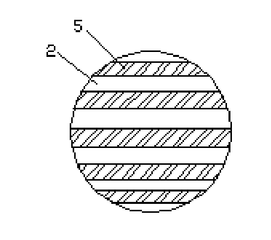
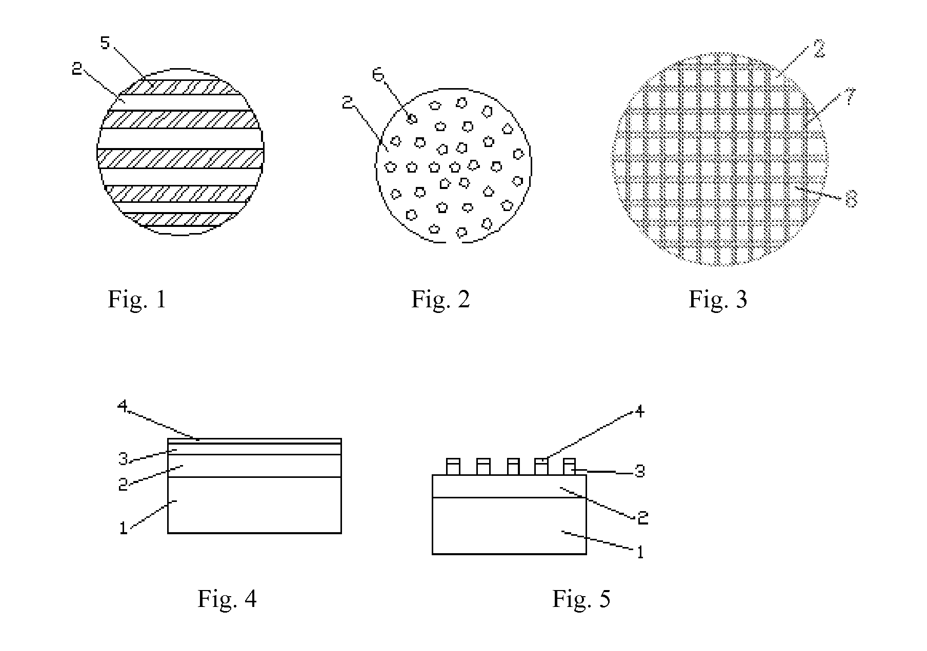
[0043]The switch contact component as shown in FIGS. 1, 4, and 5, is a small elliptic columnar granule with a three layer laminated structure, with a thickness of 3 mm and a cross sectional area of 8 mm2.

[0044]The under layer is a silicone rubber layer 1; the continuous base metal copper sheet layer 2 is sandwiched as a mid layer; and the upper layer is a bimetallic layer of striped base metal nickel plating 3 and precious metal gold plating 4. The stripe 5 is 1 mm wide and the spacing between the adjacent stripes 5 is 1.5 mm, and the thickness of the base metal plating 3 of the composite layer is 3 times the thickness of the precious metal plating 4.

[0045]The said nickel base metal plating 3 is between the base metal sheet 2 and the precious metal gold plating 4.

[0046]The upper layer thickness meets the following condition: the stripe's minimum width×th...


PUM

PropertyMeasurementUnit
thicknessaaaaaaaaaa
diametersaaaaaaaaaa
diametersaaaaaaaaaa

Abstract

A switch contact element, having a layered structure comprising three layers: the bottom layer is silicone rubber, the middle layer is a continuous base metal sheet layer, and the upper layer is a discontinuous (stripe-shaped, raised-point-shaped or lattice-shaped) precious metal plated layer or a double-metal composite layer of a discontinuous base metal plated layer and a precious metal plated layer. The thickness of the bottom layer is greater than that of the middle layer, the thickness of the middle layer is greater than that of the upper layer, and the thickness of the upper layer meets the conditions that the conductive current is greater than safe current of conductive contacts on a circuit board, and the service life of a switch for the design is ensured.

Description

TECHNICAL FIELD[0001]This invention relates to the electric contact components, which connects to circuit and is capable of conducting the circuit as used in switches, buttons or keypads in electronic industry or electric power industry.BACKGROUND OF THE INVENTION[0002]A common structure of a contact component (or a conductive pill) as used in a corresponding switch panel or keypad is as follows:[0003]A metal surface layer and an elastic material (such as a rubber layer) are bonded together. Gold, silver and other precious metals have good electrical conductivity, good chemical stability and other properties, and thus they are commonly used as the contact materials. However, their expensive prices limit their applications. The chemical stability of copper, a base metal, is not as good as a precious metal. Some base metals such as nickel, titanium, iron and their alloys, including stainless steels, having a good chemical stability, are not as ideal as precious metals with respect to ...

Claims


Application Information

Patent Timeline
Patent Type & Authority Applications(United States)
IPC IPC(8): H01H1/021H01H11/04C25D3/12C23F1/32C25D7/00C23C18/31C23F1/16H01H1/06C25D3/48
CPCH01H1/021H01H1/06H01H11/04C25D3/12H01H2201/032C25D7/00C23C18/31C23F1/16C23F1/32C25D3/48C08J5/12B32B15/06B32B15/18B32B15/20B32B25/20B32B2255/06B32B2255/20B32B2255/205B32B2255/28B32B2307/202B32B2307/714B32B2307/75B32B2457/00C25D5/022C25D5/10C25D5/12C23C18/1605C23C18/1653H01H13/785
Inventor HAN, HUISHENGZHANG, HONGMEICHEN, YUANDING, YANGWU, GUOQIANG
Owner NANTONG MEMTECH TECH
Learn More