Tamper-resistant non-volatile memory device

Active Publication Date: 2016-05-26
PANASONIC SEMICON SOLUTIONS CO LTD
View PDF12 Cites 56 Cited by
  • Summary
  • Abstract
  • Description
  • Claims
  • Application Information

AI Technical Summary

Benefits of technology

[0020]A non-volatile memory device according to an exemplary embodiment of the present disclosure includes memory cells mountable on an IC and storing data. The memory cells can be used to generate digital ID data serving as entity identification information, and thus no area overhead occurs. The digital ID data is securely and stably generated and is very difficult to duplicate. Accordingly, it may be possible to provide a scheme based on PUF technology that has high resistance to side-channel attacks constituting recent serious

Problems solved by technology

However, technological advances have lead to a rapid growth of concerns about the direct interception of inside information on circuitry from outside parties.
However, such standards, which are regarded as being safe in providing protection against hacking of encrypted data, have still involved a concern for vulnerability of the encryption key to direct hacking.
The former configuration has experienced a problem that permits the state of the fuse element to be observed using X-ray projection or the like and the electrical conductivity of the fuse element to be analyzed, resulting in the stored key information being hacked or stolen.
The latter configuration does not lead to analysis by using X-ray projection but has a problem in that the key information can be hacked by direct application of probes to both ends of a memory element of the non-volatile memory to electrically read the state of the element.
However, techniques called side-channel attacks, which have been attempting to break the countermeasure described above, can constitute threats.
These techniques are threats because such techniques enable an attacker (or hacker) to hack key information without causing any physical damage to an IC when the IC is in actual operation.
Since it is not possible to artificially control the physical properties of each IC, data whose physical duplication is not possible can be generated.
In actual use, however, specific entity identification information determined

Method used


Image

  • Tamper-resistant non-volatile memory device
  • Tamper-resistant non-volatile memory device
  • Tamper-resistant non-volatile memory device

Examples


Example

First Embodiment

Overview of Non-Volatile Resistive Memory Device According to Embodiment of Present Disclosure

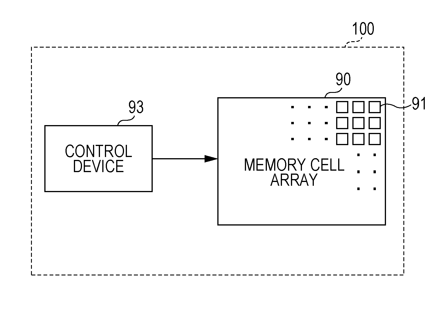
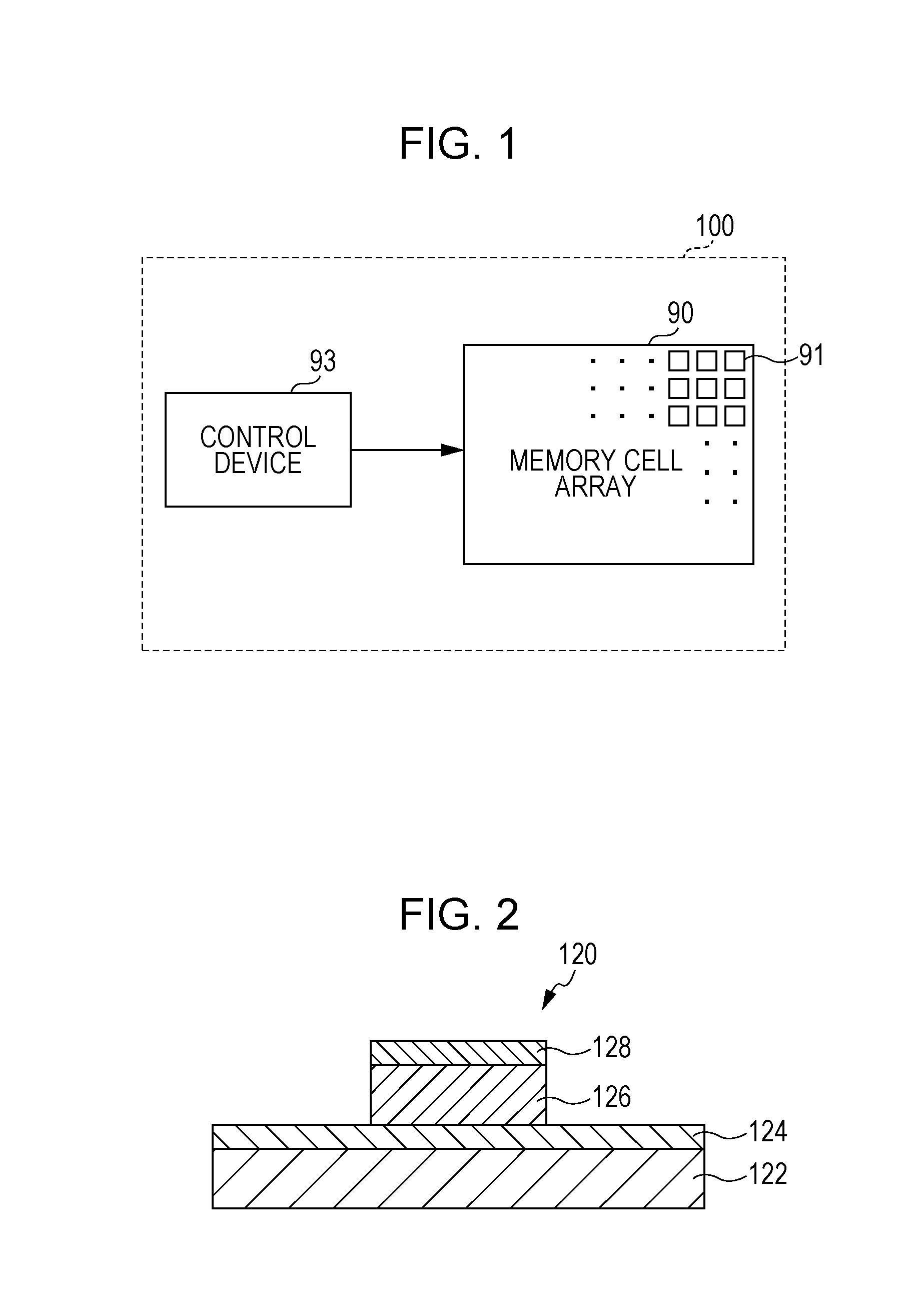
[0124]FIG. 1 is a block diagram illustrating an example of the schematic configuration of a non-volatile resistive memory device 100 according to a first embodiment. FIG. 2 is a cross-sectional view illustrating an example of the schematic configuration of a memory cell included in the non-volatile resistive memory device 100 according to the first embodiment.

[0125]In the example illustrated in FIG. 1, the non-volatile resistive memory device 100 according to this embodiment at least includes a memory cell array 90 and a control device 93. The control device 93 may not necessarily be included in the non-volatile resistive memory device 100, and a control device located outside the non-volatile resistive memory device 100 may be connected to the non-volatile resistive memory device 100 and used to perform the following operation.

[0126]The memory cell array 90 has a configurat...


PUM


Abstract

A non-volatile memory device includes a memory cell array including memory cells, a read circuit that, in operation, obtains pieces of resistance value information each relating to the resistance value of one of the memory cells, an arithmetic circuit that, in operation, calculates a binary reference value based on at least a part of the pieces of resistance value information, and a data adjustment circuit. In operation, the read circuit assigns, based on the binary reference value, 0 or 1 to each of the pieces of resistance value information. In operation, the data adjustment circuit determines whether to adjust the binary reference value, in accordance with a difference between the numbers of pieces of digital data “0” and digital data “1” in the pieces of digital data.

Description

BACKGROUND[0001]1. Technical Field[0002]The present disclosure relates to a tamper-resistant non-volatile memory device including a plurality of non-volatile resistive memory cells.[0003]2. Description of the Related Art[0004]The market for electronic commerce services rendered via the Internet, such as electronic banking or electronic shopping, is rapidly expanding. Such services are paid for with electronic methods of payment like electronic money using integrated circuit (IC) cards and smartphone terminals whose use is also expanding. These services require high-level security technology for mutual authentication during communication and encryption of communication data all the time in order to make payment safe.[0005]In terms of software technologies, due to the accumulation of encryption techniques based on program processing, such as high-level encryption algorithms, a sufficient level of security has been achieved. However, technological advances have lead to a rapid growth o...

Claims


Application Information

Patent Timeline
IPC IPC(8): G11C13/00
CPCG11C13/004G11C2013/0054G11C13/0097G11C13/0069G09C1/00G11C13/0007G11C13/0059G11C16/20G11C2013/0073G11C2013/0083H04L2209/12
Inventor YOSHIMOTO, YUHEIKATOH, YOSHIKAZU
Owner PANASONIC SEMICON SOLUTIONS CO LTD
Why Eureka
Try Eureka