Conductive film, touch panel and display device employing same, and evaluation method for electrically conductive film

a conductive film and touch panel technology, applied in the direction of shielding materials, instruments, computing, etc., can solve the problems of inability to disclose the correspondence between pseudo random change and suppression of moire, and insufficient improvement of visibility of moire. , to achieve the effect of suppressing the generation of moire, noise, and improving the visibility of moir

Active Publication Date: 2016-06-16
FUJIFILM CORP
View PDF8 Cites 22 Cited by
  • Summary
  • Abstract
  • Description
  • Claims
  • Application Information

AI Technical Summary

Benefits of technology

[0049]As described above, according to the invention, it is possible to suppress the generation of moire, regardless of the observation distance from a display screen of a display unit and to improve the visibility of moire which is inevitable in principle using a noise effect. As a result, it is possible to improve the visibility of moire and noise and thus to significantly improve the visibility of the display screen.
[0050]According to the invention, particularly, it is possible to suppress the generation of moire that causes large deterioration of image quality when a transparent conductive film having wiring lines is used as a touch panel electrode and is superimposed on a black matrix of a display unit of a display device, regardless of the observation distance, to improve the visibility of moire which is inevitable in principle, make it difficult for an observer to perceive the granularity of noise, to obtain sufficient transmittance, and to significantly improve display visibility on a touch panel.
[0051...

Problems solved by technology

As a result, the visibility of moire is not sufficiently improved.
As a result, there is a problem in that the visual recognition of moire due to intensity is promoted and the visibility of moire is insufficiently improved.
However, the technique merely aims to reduce the feeling of noise of the mesh pattern in the transparent conductive film and does not lead to the suppression of moire generated between the BM pattern of the display...

Method used


Image

  • Conductive film, touch panel and display device employing same, and evaluation method for electrically conductive film
  • Conductive film, touch panel and display device employing same, and evaluation method for electrically conductive film
  • Conductive film, touch panel and display device employing same, and evaluation method for electrically conductive film

Examples


examples

[0230]Hereinafter, the invention will be described in detail with reference to examples.

[0231]For example, materials, the amounts used, proportions, the content of processes, and the procedure of the processes described in the following examples can be appropriately changed without departing from the scope and spirit of the invention. That is, the scope of the invention should not be construed as being limited by the following examples.

first example

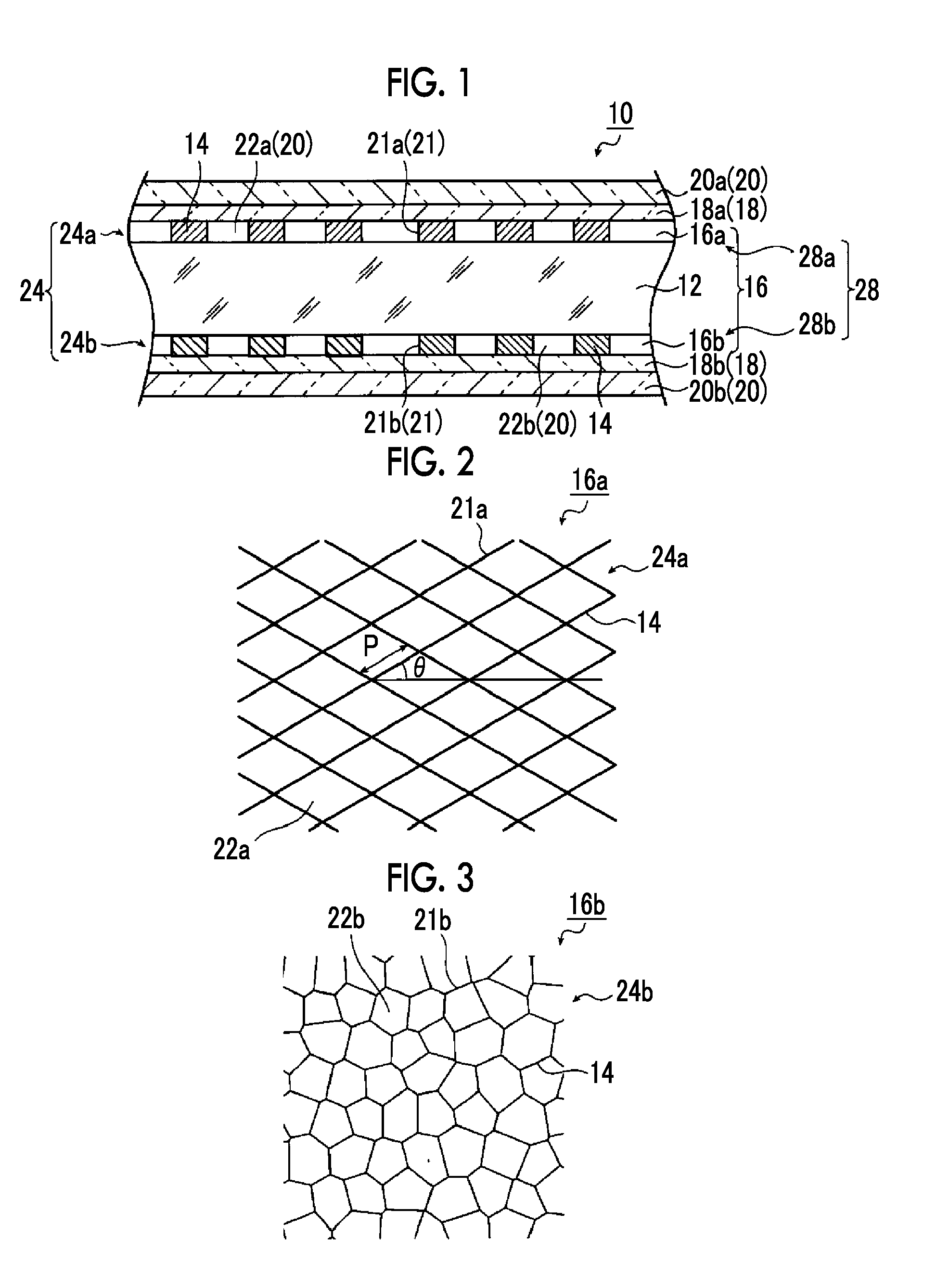
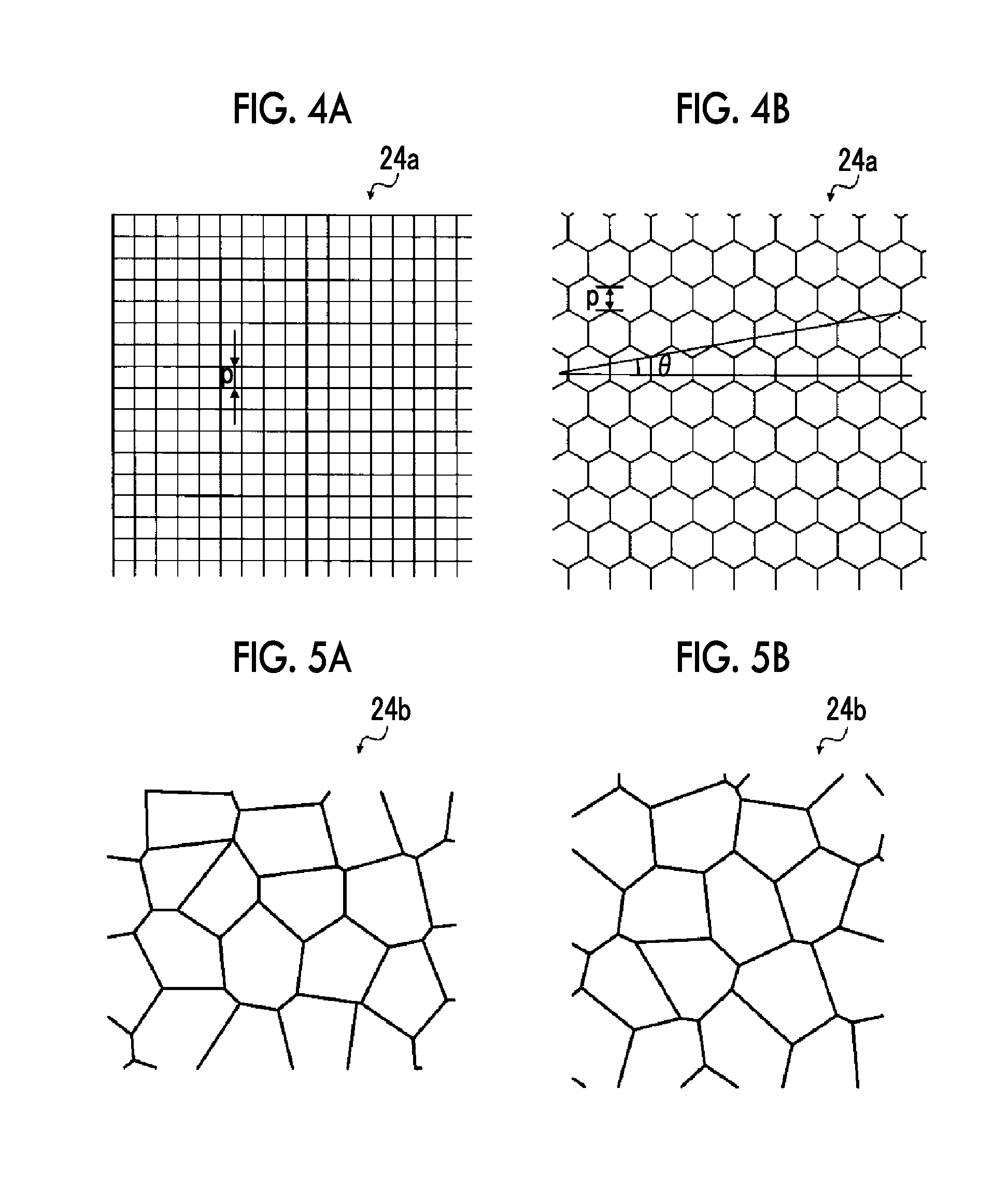
[0232]For the BM pattern 38 illustrated in FIG. 11(A) and the conductive film 10 according to the first embodiment having a composite wiring pattern, which was a combination of the wiring pattern 24b as an irregular pattern illustrated in FIG. 16(A) and the wiring pattern 24a as a regular pattern illustrated in FIG. 16(C), the combination of the wiring patterns 24a and 24b was changed to various combinations with different pattern regularities and the combination of the wiring patterns 24a and 24b and the BM pattern 38 were superimposed on each other in simulation samples and the actual samples. Then, the quantitative value of moire was calculated and three researchers performed visual sensory evaluation for moire which was generated due to the interference between the two superimposed patterns.

[0233]The sensory evaluation results were represented by three levels ◯(1), Δ(2), and x (3). When all of three researches evaluated that moire did not cause discomfort, ◯(1) indicating that t...

second example

Silver Halide Photosensitive Material

[0247]An emulsion which included 10.0 g of gelatin with respect to 150 g of Ag in an aqueous medium and contained iodobromochloride silver particles (I=0.2 mol %, Br=40 mol %) having an average sphere-equivalent diameter of 0.1 vim was produced.

[0248]K3Rh2Br9 and K2IrCl6 were added to the emulsion such that concentration was 10−7 (mol / mol Ag) to dope silver bromide particles with Rh ions and Ir ions. In addition, Na2PdCl4 was added to the emulsion and old-sulfur sensitization was performed for the emulsion using chloroauric acid and sodium thiosulfate. Then, a gelatin hardening agent and the emulsion were applied onto a base (here, on polyethylene terephthalate (PET)) such that the amount of silver applied was 10 g / m2. At that time, the volume ratio of Ag to gelatin was 2 / 1.

[0249]The emulsion was applied with a width of 25 cm and a length of 20 m onto a PET support with a width of 30 and each of both ends of the support was cut by 3 cm such that ...


PUM


Abstract

First and second wiring patterns which are formed on both surfaces of a base have first and second patterns which are different from each other, respectively, and are superimposed as a composite wiring pattern on a pixel array pattern. A plurality of spectrums in a two-dimensional Fourier space of transmittance image data of the pixel array pattern and the composite wiring pattern are excluded from a plurality of spectrums in a two-dimensional Fourier space of transmittance image data of a composite pattern of the pixel array pattern and the composite wiring pattern to extract a plurality of spectrums of only noise and moire generated by interference between the pixel array pattern and the composite wiring pattern. The sum of all of the extracted plurality of spectrums is calculated and an extraction quantitative value of the moire and the noise calculated from the sum is in a predetermined range.

Description

CROSS-REFERENCE TO RELATED APPLICATIONS[0001]This application is a Continuation of PCT International Application No. PCT / JP2014 / 072518 filed on Aug. 28, 2014, which claims priority under 35 U.S.C. §119(a) to Japanese Application No. 2013-180708 filed on Aug. 30, 2013. The above application is hereby expressly incorporated by reference, in its entirety, into the present application.BACKGROUND OF THE INVENTION[0002]1. Field of the Invention[0003]The present invention relates to a conductive film, a touch panel and a display device including the conductive film, and a conductive film evaluation method, and more particularly, to a conductive film having mesh pattern wires that is excellent regarding the visibility of moire and noise in the design of a mesh wiring pattern (hereinafter, referred to as a mesh pattern) in which a plurality of opening portions (cells) are formed by a plurality of thin metal wires, a touch panel and a display device including the conductive film, and a conduc...

Claims


Application Information

Patent Timeline
IPC IPC(8): G06F3/041G06F3/044H05K9/00
CPCG06F3/0412H05K9/0096G06F2203/04112G06F3/044H05K9/009G06F3/0445G06F3/0446
Inventor IWAMI, KAZUCHIKA
Owner FUJIFILM CORP
Why Eureka
Try Eureka