Method and Apparatus for Reviewing Defects
a technology of defects and apparatus, applied in the direction of instruments, semiconductor/solid-state device testing/measurement, nuclear engineering, etc., can solve the problems of increased equipment cost, increased equipment cost, and reduced throughput, and achieve high accuracy
- Summary
- Abstract
- Description
- Claims
- Application Information
AI Technical Summary
Benefits of technology
Problems solved by technology
Method used
Image

Examples
embodiment 1
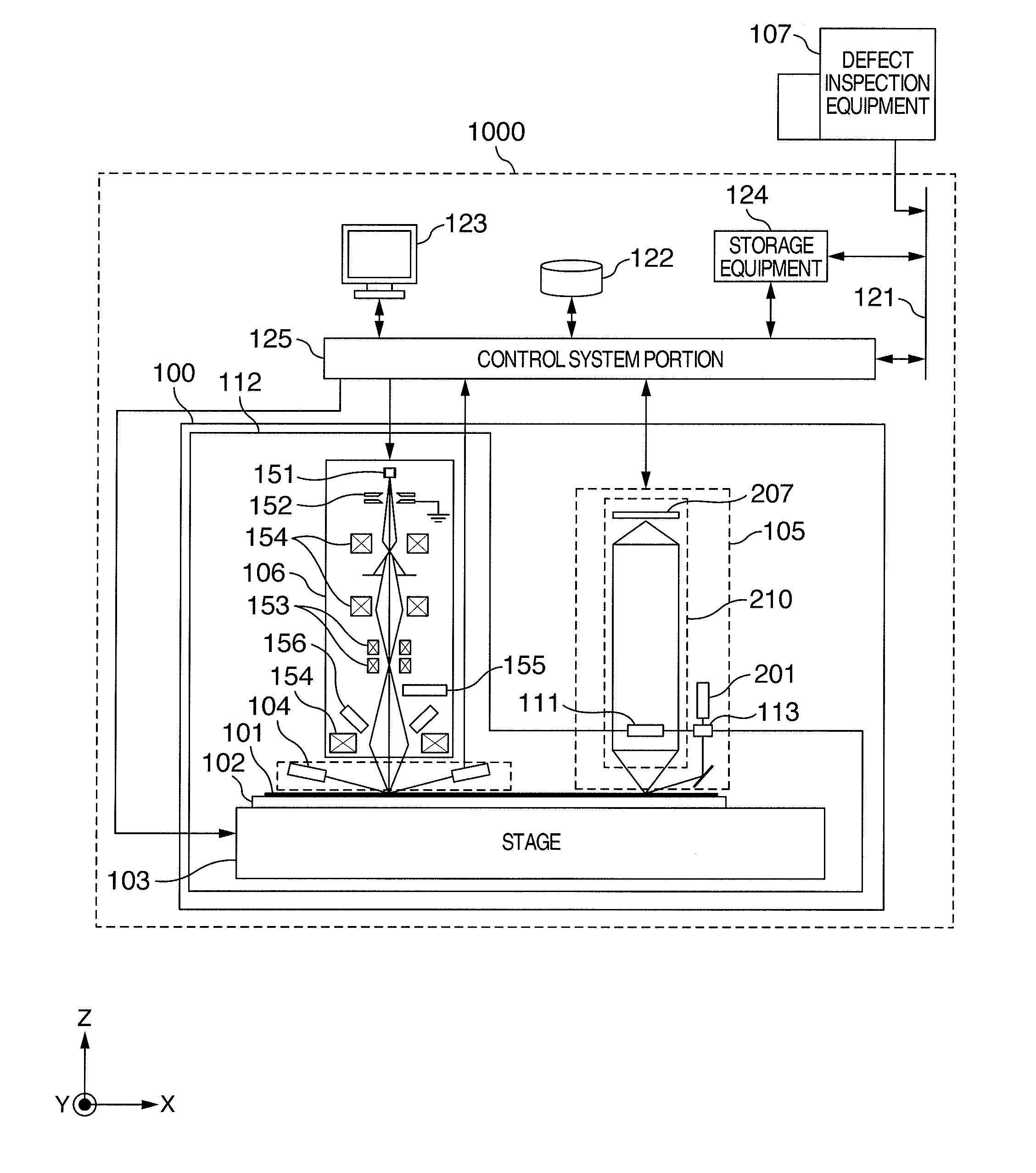
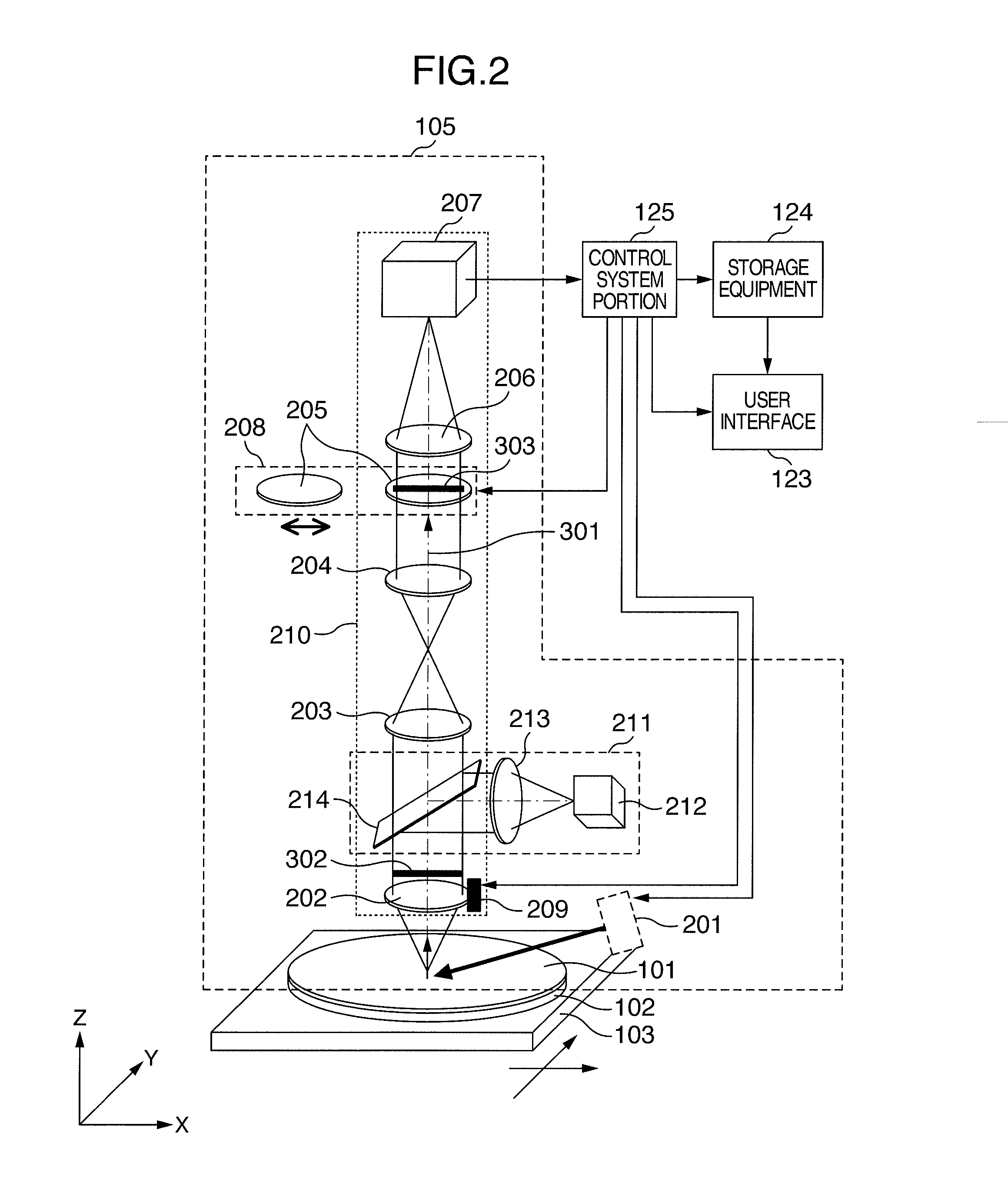
[0019]FIG. 1 is a construction diagram of a defect reviewing apparatus according to Embodiment 1 of the present invention. A defect reviewing apparatus 1000 includes in general a reviewing equipment 100, a network 121, a database 122, a user interface 123, a storage equipment 124, and a control system portion 125. Furthermore, the defect reviewing apparatus 1000 is connected via the network 121 to a defect inspecting equipment 107 as another inspection equipment.
[0020]The defect inspecting equipment 107 detects a defect that exists on a sample 101 and acquires defect information such as position coordinates and a size of the defect. The defect inspecting equipment 107 only needs to be one which can acquire information regarding a defect that exists on a sample 101.
[0021]The defect information acquired by the defect inspecting equipment 107 is input to the storage equipment 124 or the control system portion 125 via the network 121. The storage equipment 124 stores the defect informat...
embodiment 2
[0066]Next, Embodiment 2 will be described. Since a construction of a reviewing apparatus according to the present embodiment is the same as shown in FIGS. 1 to 3, its description will be omitted. The present embodiment is different from Embodiment 1 in that the inspection modes can be automatically set based on defect information.
[0067]With reference to FIG. 5, a flow of a defect reviewing process according to Embodiment 2 will be described. Detailed description of the steps with the same reference numerals as those in FIG. 4 will be omitted.
[0068]S320: After reading defect information (S300), setting a wafer (S301), performing a coarse alignment (S302), and moving a defect in the field of view of the optical microscope portion 105 (S305), the size of a defect to be reviewed is determined. At this point, when the size of the defect to be reviewed is minute and smaller than a preset threshold (S320—smaller than threshold value), the high sensitivity inspection mode is automatically ...
embodiment 3
[0073]Next, Embodiment 3 according to the present invention will be described. Since a construction of a reviewing apparatus according to the present embodiment is the same as shown in FIGS. 1 to 3, its description will be omitted. The present embodiment is different from Embodiment 1 in that the inspection method in repeated search after the first detection of a defect has been unsuccessful in the optical microscope portion.
[0074]With reference to FIG. 7, a flow of a defect reviewing process according to Embodiment 3 will be described. Since the steps from reading the defect information (S300) to searching for a defect (S307) are the same as those shown in FIG. 4, their description will be omitted.
[0075]S330: When the defection of the defect has been unsuccessful (S308 unsuccessful), the inspection mode is changed. An explanation is given for the case where the high sensitivity inspection mode has been set, for example, at the time of inspection mode setting (S303). When the detect...
PUM
 Abstract
Description
Claims
Application Information
 - R&D
- Intellectual Property
- Life Sciences
- Materials
- Tech Scout
- Unparalleled Data Quality
- Higher Quality Content
- 60% Fewer Hallucinations
Browse by: Latest US Patents, China's latest patents, Technical Efficacy Thesaurus, Application Domain, Technology Topic, Popular Technical Reports.
© 2025 PatSnap. All rights reserved.Legal|Privacy policy|Modern Slavery Act Transparency Statement|Sitemap|About US| Contact US: help@patsnap.com