
Group iv nanowires grown from inductively or resistively heated substrates

a technology of inductive heating and nanowires, applied in the field of group iv nanowires, can solve the problems of affecting the performance of nanowires, affecting the quality of nanowires, and most synthesis methods cannot be realized at a commercially significant scale, so as to improve the growth of nanowires, reduce processing time, and rapidly produce a large quantity of high-quality nanowires

Inactive Publication Date: 2016-08-18
CORNELL UNIVERSITY
View PDF0 Cites 5 Cited by
  • Summary
  • Abstract
  • Description
  • Claims
  • Application Information

AI Technical Summary

Benefits of technology

This patent describes a method of growing crystalline nanowires on a metal substrate using resistive or inductive heating. This method can be used to produce high-quality nanowires in a positive or atmospheric pressure environment without the need for expensive equipment or processing time. The resulting nanowires can be used for various applications such as in lithium-ion batteries. The method is also adaptable to roll-to-roll processing, which allows for the production of material for the anode component of batteries. The patent also describes a method for attaching different functional groups to the nanowires to enable various applications. Overall, the method is efficient, flexible, and cost-effective.

Problems solved by technology

However, most synthesis methods cannot be realized at a commercially significant scale (i.e., greater than kg / day).
This method produces commercially significant yields of nanowires, but commercial production of the noble metal seeds, extraction of the nanowires, and post-processing cause complications.
The current methods of attachment are sub-optimal and hinder nanowire performance.
This causes unnecessary heating of the reaction fluid that is not in contact with the surface, which wastes heat and precursor.
In addition heating the entire environment results in no discrimination as to where the nanowire reaction occurs, so patterned growth is difficult or even impossible.

Method used

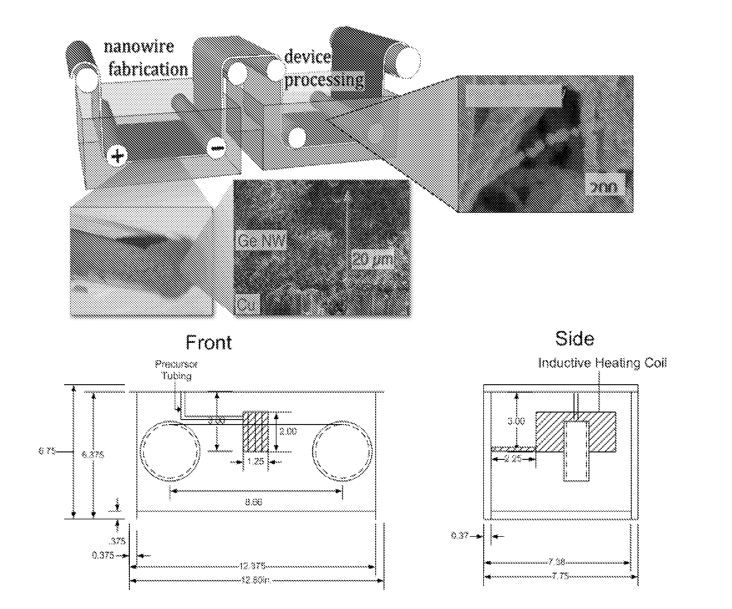
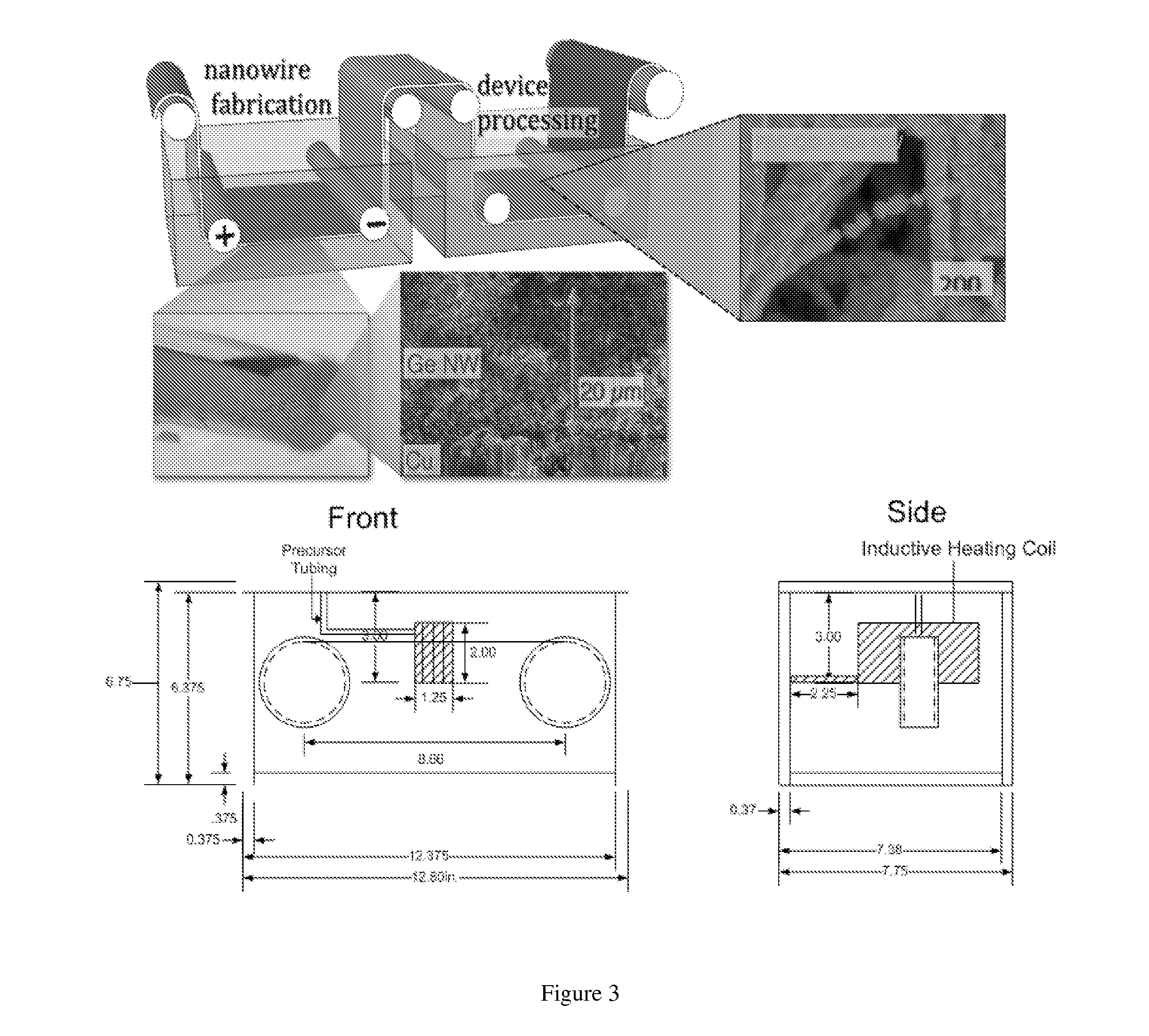

Image

  • Group iv nanowires grown from inductively or resistively heated substrates
  • Group iv nanowires grown from inductively or resistively heated substrates
  • Group iv nanowires grown from inductively or resistively heated substrates

Examples


working examples

Example 1

Liquid Phase Reaction—Si

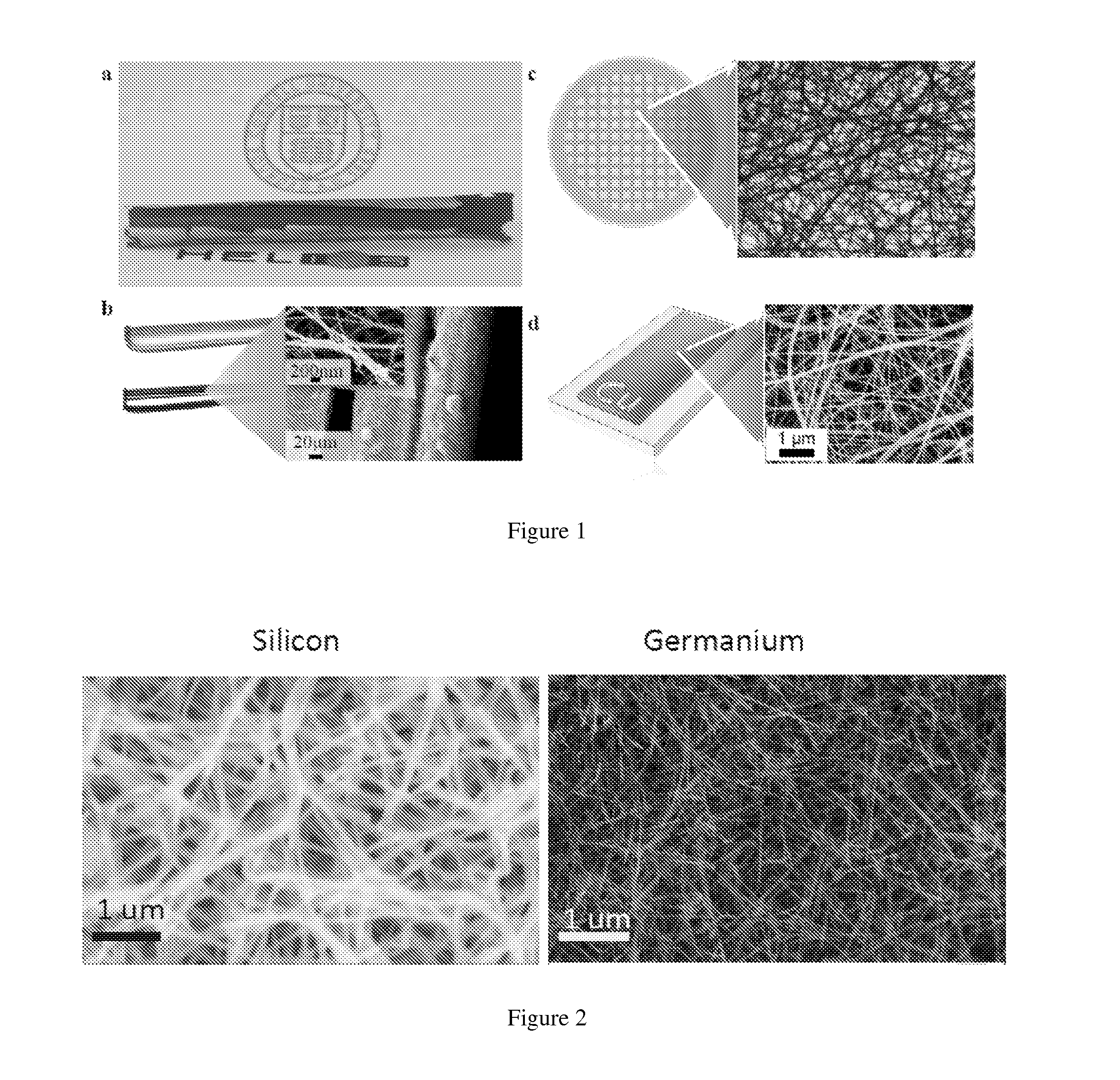
[0085]The patterned geometry (thickness of Cu 100 nm) in FIG. 9 was attached to a power supply and placed in a solution of 100 mM trisilane and squalene. The power supply provided 2.1*107 W / m2 of resistive heating. The reaction lasted seconds. This created the nanowires observed in FIG. 10.

example 2

Liquid Phase Reaction—Ge

[0086]The patterned geometry (thickness of Cu 100 nm) in FIG. 10 above was attached to a power supply and placed in a solution of 100 mM diphenylgermane and squalene. The power supply provided 3*107 W / m2 of resistive heating. The reaction lasted 2.5 minutes. This created the nanowires observed in FIG. 11.

example 3

Vapor Phase Reaction—Si

[0087]The patterned geometry (thickness of Cu 100 nm) in FIG. 9 was attached to a power supply and placed above 300 μl of trisilane in a nitrogen environment. The power supply provided 6*106 W / m2 of resistive heating. The reaction lasted ten seconds. This created the nanowires observed in FIG. 12. This, by extension, should be applicable to Ge nanowires.


PUM

PropertyMeasurementUnit
temperatureaaaaaaaaaa
reaction timeaaaaaaaaaa

Abstract

Growth of Group IV nanowires with a substrate and a Group IV metalloid is performed using resistive or inductive heating of the substrate. A roll-to-roll process enables a metal surface to move through a reaction environment while reacting with a stream or bath of precursor to form the nanowire-metal complex. The Group IV nanowires on a surface of the substrate can have a surface loading greater than 10 mg / cm2.

Description

CROSS-REFERENCE TO RELATED APPLICATIONS[0001]This application claims priority to the provisional patent application assigned U.S. App. No. 61 / 889,745 and filed Oct. 11, 2013, the disclosure of which is hereby incorporated by reference.STATEMENT REGARDING FEDERALLY-SPONSORED RESEARCH OR DEVELOPMENT[0002]This invention was made with government support under Grant Number DE-FG02-87ER45298 awarded by the Department of Energy. The government has certain rights in the invention.FIELD OF THE DISCLOSURE[0003]This disclosure relates to Group IV nanowires and, more particularly, to a method of making Group IV nanowires.BACKGROUND OF THE DISCLOSURE[0004]Nanowires have the potential to be the base material for a broad range of next-generation applications. Their one-dimensional structure gives rise to many unique physical, optical and electrical characteristics that can be applied to a broad spectrum of applications such as, for example, transistors, fuel cells, water splitting, stealth applica...

Claims


Application Information

Patent Timeline
Patent Type & Authority Applications(United States)
IPC IPC(8): C30B23/06C23C18/12B22F1/00B22F1/02C25D3/38C25D7/06C30B7/12C30B7/14C30B25/10C30B30/02C30B29/62C30B29/06C30B29/08C30B29/52C30B29/02C23C14/16B22F1/18
CPCC25D3/38C30B7/12C23C18/06C23C18/08C23C18/1204C23C18/1241C23C18/1291C23C14/16C23C14/562C30B29/06C30B29/08C30B29/60C30B33/00B22F1/0025B22F1/025C30B29/02C30B25/10C30B23/063C30B7/14C30B30/02C23C18/1262C30B29/62C30B29/52C25D7/0614B22F1/0547B22F1/18
Inventor HANRATH, TOBIASRICHARDS, BENJAMIN T.
Owner CORNELL UNIVERSITY
Learn More