Image-capturing device, radiation detection apparatus, and control method for image-capturing device
- Summary
- Abstract
- Description
- Claims
- Application Information
AI Technical Summary
Benefits of technology
Problems solved by technology
Method used
Image
Examples
first embodiment
1. First Embodiment
“Example of Configuration of Semiconductor Light Detection Apparatus”
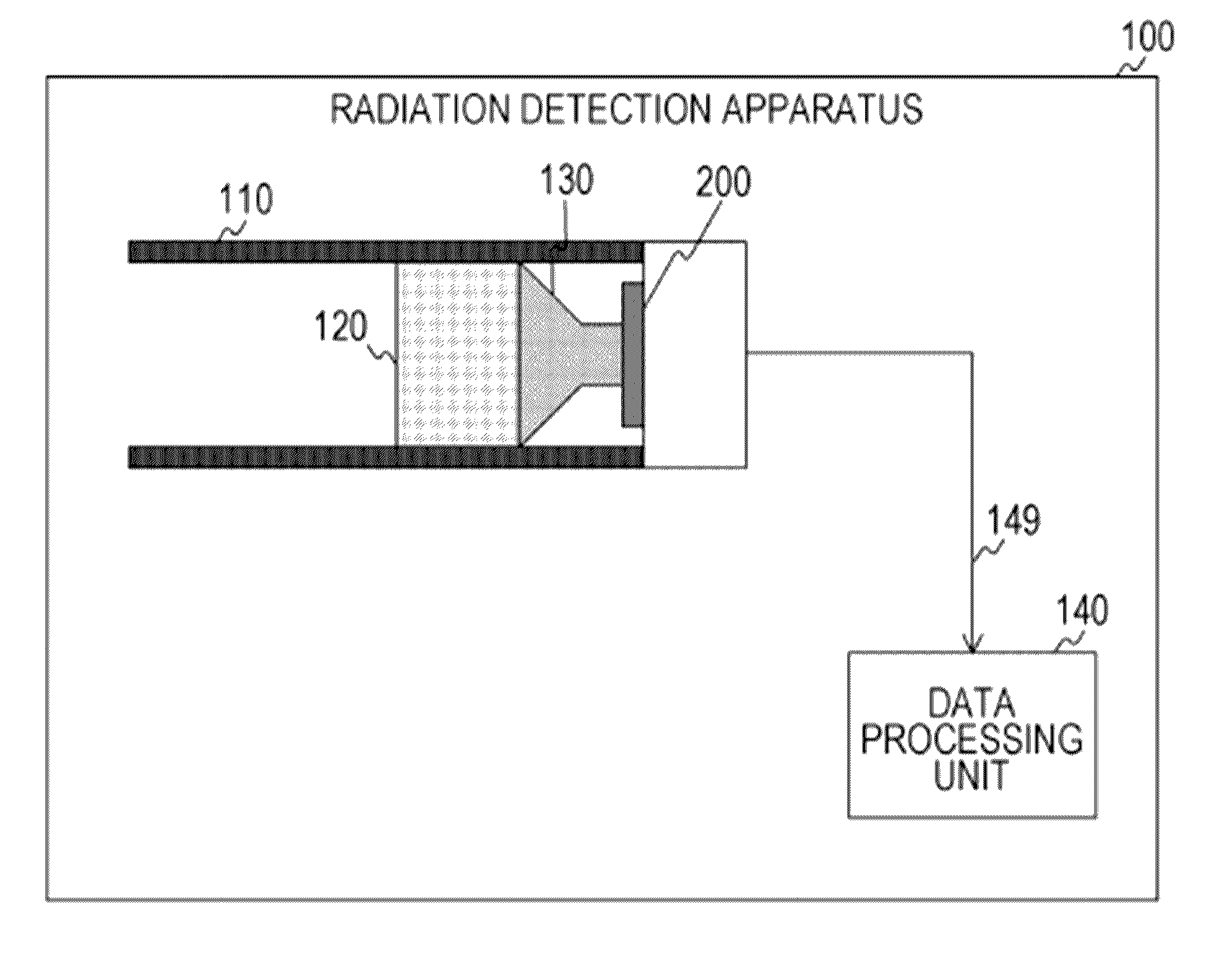
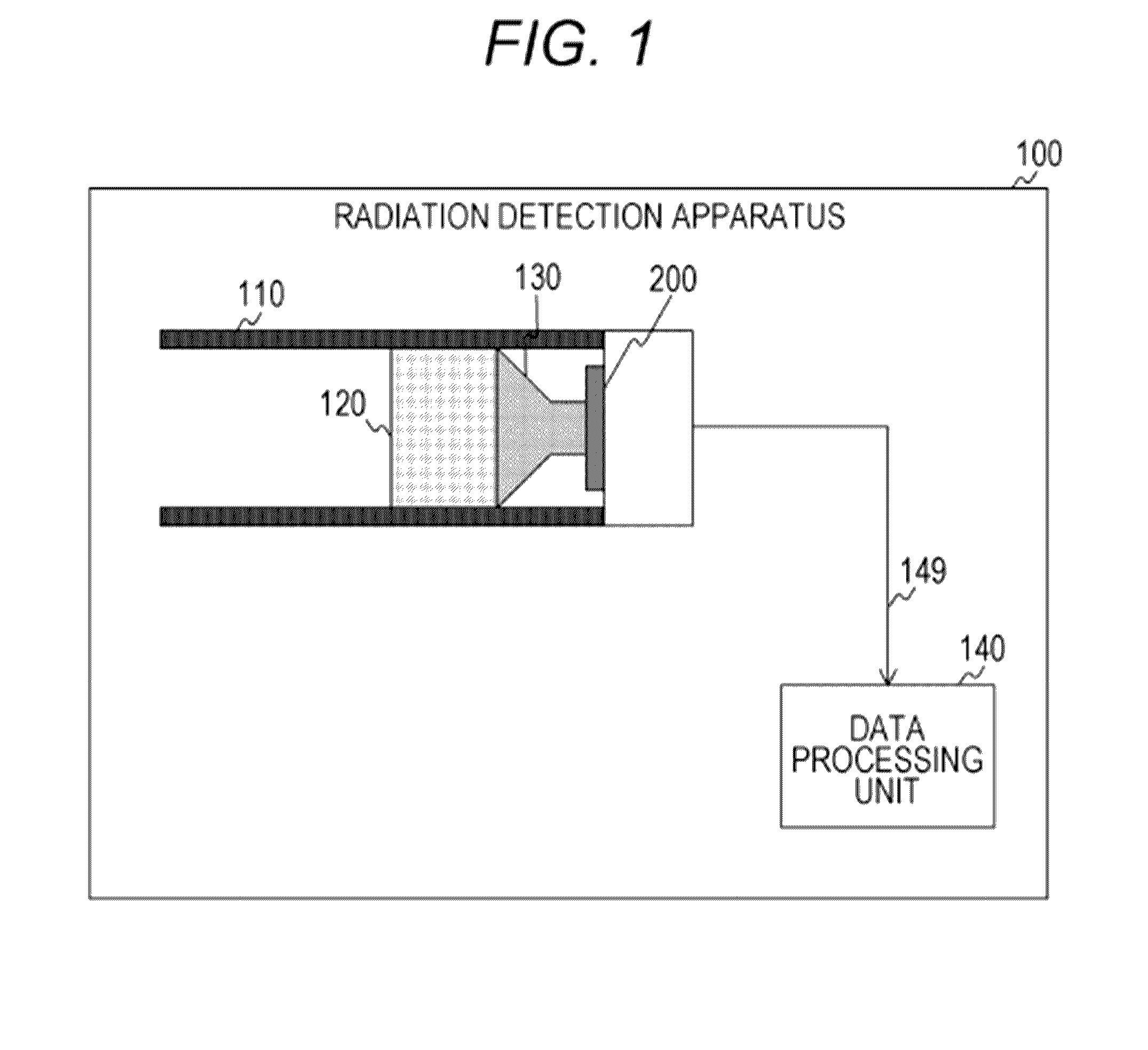
[0061]FIG. 1 is a block diagram illustrating an example of a configuration of a radiation detection apparatus 100 according to the first embodiment. This radiation detection apparatus 100 includes a collimator 110, a scintillator 120, an optical guide 130, an image-capturing device 200, and a data processing unit 140.
[0062]The collimator 110 is configured to pass only the radiation incident upon the image-capturing device 200 in a direction perpendicular thereto. This collimator 110 is made of, for example, lead. The radiation that has passed through the collimator 110 enters the scintillator 120.
[0063]The scintillator 120 receives the radiation that has passed through the collimator 110 and emits scintillation light. The optical guide 130 condenses the scintillation light and guides the scintillation light to the image-capturing device 200. This optical guide 130 also has a light homogenization ...
second embodiment
2. Second Embodiment
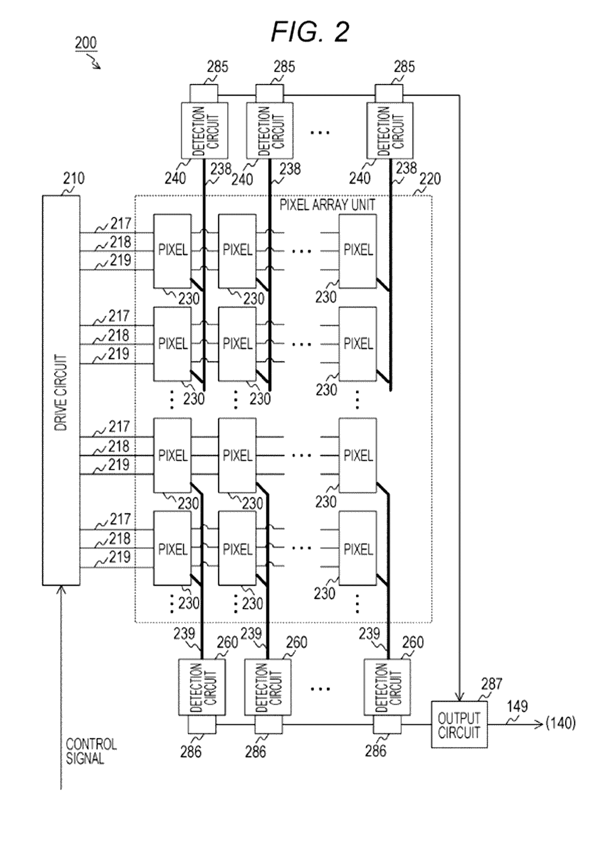
[0163]In the first embodiment explained above, the image-capturing device 200 exposes multiple sections one by one in order, and in that case, the number of pixels exposed at a time is 64 pixels in two rows, and the light incident upon the other pixels is not detected. Or when detection result of each of 64 pixels for a single exposure is binary-determined, 64 is 26, and therefore, only six-bit gradation level is obtained in the energy detection. More specifically, in the configuration for exposing each section in order, the dynamic range of the energy detection is poor, and the dynamic range is limited by the number of pixels exposed at a time.
[0164]Therefore, a mechanism for performing exposure in an extremely short period of time at a time in multiple sections is required. This corresponds to a so-called global shutter operation in a CMOS image sensor. By exposing multiple sections at a time, many pixels can be used for light detection without increasing the c...
third embodiment
3. Third Embodiment
[0203]In the second embodiment explained above, the pixels 230 and the detection circuits 260 are provided on the same substrate. Alternatively, pixels may be provided on one of two substrates stacked by three dimensional silicon stacking technique, and detection circuits may be provided on the other of the two substrates. The radiation detection apparatus 100 according to the third embodiment is different from the first embodiment in that the pixels are provided on one of the two stacked substrates, and the detection circuits are provided on the other of the two substrates.
[0204]FIG. 17 is a perspective view illustrating an example of a configuration of a radiation detection apparatus 100 according to the third embodiment. The radiation detection apparatus 100 according to the third embodiment is different from the first embodiment in that multiple scintillator devices 121 and an image-capturing device 201 are provided instead of the scintillator 120, the optical...
PUM
 Abstract
Description
Claims
Application Information


