Negative supply rail positive boost write-assist circuits for memory bit cells employing a p-type field-effect transistor (PFET) write port(s), and related systems and methods

a write-assist circuit and negative supply rail technology, applied in the field of memory systems, can solve problems such as and achieve the effects of reducing memory write times, improving memory performance, and reducing the effective mass of charge carriers

Inactive Publication Date: 2016-08-25
QUALCOMM INC
View PDF4 Cites 12 Cited by
  • Summary
  • Abstract
  • Description
  • Claims
  • Application Information

AI Technical Summary

Benefits of technology

[0009]Aspects of the disclosure involve write-assist circuits for memory bit cells (“bit cells”) employing a P-type Field-Effect transistor (PFET) write port(s). Related methods and systems are also disclosed. The bit cells are provided in a data array of a memory system in a processor-based system to store data. It has been observed that as node technology is scaled down in size, PFET drive current (i.e., drive strength) exceeds N-type Field-Effect transistor (NFET) drive current for like-dimensioned FETs. This is due to the introduction of strained silicon in FET fabrication to reduce the effective mass of charge carriers. A write port is a performance critical element in a bit cell. In this regard, in one aspect, it is desired to provide bit cells having PFET write ports, as opposed to NFET write ports, to reduce memory write times to the bit cells, and thus improve memory performance. To mitigate a write contention that could otherwise occur when writing data to bit cells, write-assist circuits are provided for bit cells having a PFET write port(s). By mitigating or avoiding write contention issues in the bit cells, the voltage supply providing the minimum voltage to the bit cells for operation and data retention can be reduced to reduce power consumption and increase processor energy efficiency.

Problems solved by technology

This is due to the introduction of strained silicon in FET fabrication to reduce the effective mass of charge carriers.

Method used


Image

  • Negative supply rail positive boost write-assist circuits for memory bit cells employing a p-type field-effect transistor (PFET) write port(s), and related systems and methods
  • Negative supply rail positive boost write-assist circuits for memory bit cells employing a p-type field-effect transistor (PFET) write port(s), and related systems and methods
  • Negative supply rail positive boost write-assist circuits for memory bit cells employing a p-type field-effect transistor (PFET) write port(s), and related systems and methods

Examples


Embodiment Construction

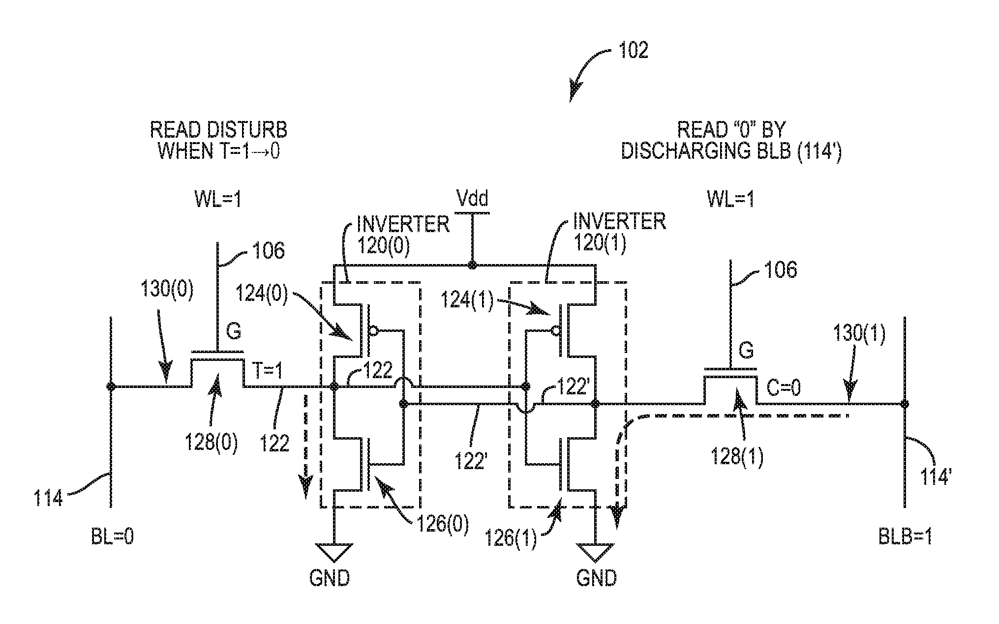
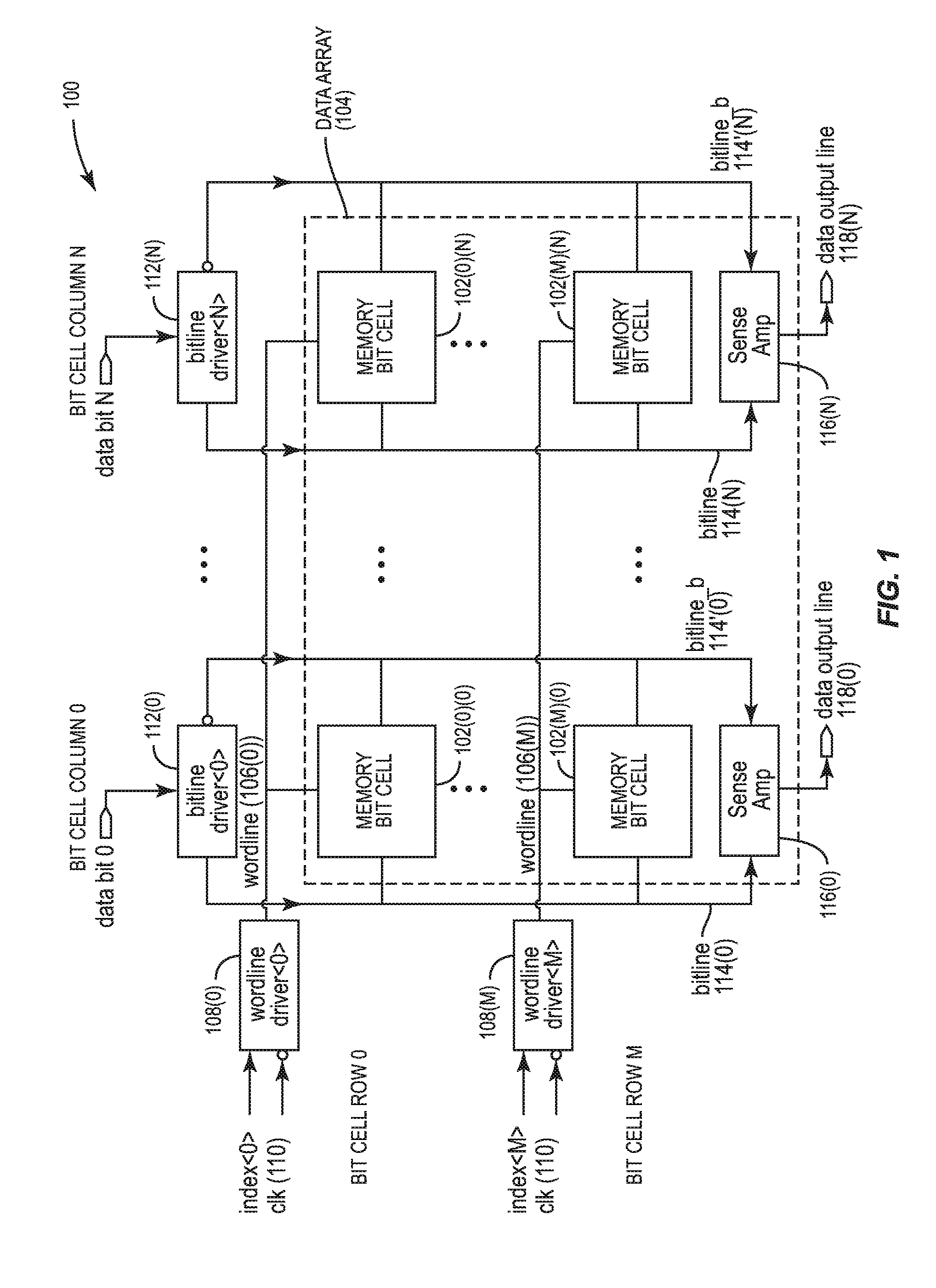
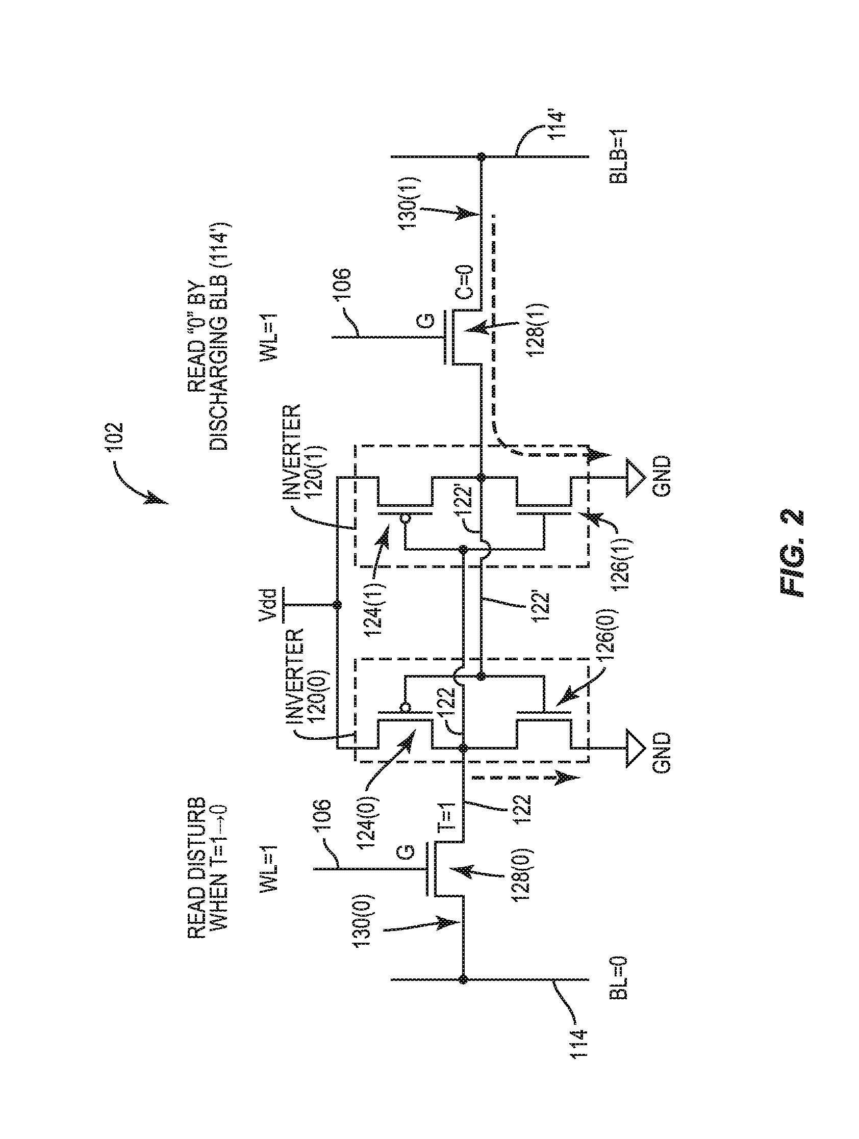
[0028]With reference now to the drawing figures, several exemplary aspects of the present disclosure are described. The word “exemplary” is used herein to mean “serving as an example, instance, or illustration.” Any aspect described herein as “exemplary” is not necessarily to be construed as preferred or advantageous over other aspects.

[0029]Memory bit cells are provided in a data array of a memory system in a processor-based system to store data. As shown in a graph 400 in FIG. 4, it has been observed that as node technology is scaled down in size, P-type Field-Effect Transistor (PFET) drive current (i.e., drive strength) exceeds N-type Field-Effect transistor (NFET) drive current for like-dimensioned FETs. This is due to the introduction of strained silicon in FET fabrication to reduce the effective mass of charge carriers. As illustrated in FIG. 4, the technology node size in nanometers (nm) is provided on an X-axis 402. The ratio of a saturation drain current of a PFET (IDSAT, N...


PUM


Abstract

Write-assist circuits for memory bit cells (“bit cells”) employing a P-type Field-Effect transistor (PFET) write port(s) are disclosed. Related methods and systems are also disclosed. It has been observed that as node technology is scaled down in size, PFET drive current (i.e., drive strength) exceeds N-type Field-Effect transistor (NFET) drive current for like-dimensioned FETs. In this regard, in one aspect, it is desired to provide bit cells having PFET write ports, as opposed to NFET write ports, to reduce memory write times to the bit cells, and thus improve memory performance. To mitigate a write contention that could otherwise occur when writing data to bit cells, a write-assist circuit provided in the form of a negative supply rail positive boost circuit can be employed to weaken an NFET pull-down transistor in a storage circuit of a memory bit cells having a PFET write port(s).

Description

PRIORITY APPLICATION[0001]The present application claims priority under 35 U.S.C. §119(e) to U.S. Provisional Patent Application Ser. No. 62 / 119,763 filed on Feb. 23, 2015 and entitled “WRITE-ASSIST CIRCUITS FOR MEMORY BIT CELLS EMPLOYING A P-TYPE FIELD-EFFECT TRANSISTOR (PFET) WRITE PORT(S), AND RELATED SYSTEMS AND METHODS,” which is incorporated herein by reference in its entirety.BACKGROUND[0002]I. Field of the Disclosure[0003]The technology of the disclosure relates generally to memory systems employing addressable static memory bit cells for reading and writing data, and more particularly to write-assist circuits for mitigating write contention conditions when writing to bit cells.[0004]II. Background[0005]Supply voltage (i.e., Vdd) scaling is an effective technique for maximizing processor energy efficiency across all market segments, ranging from small, embedded cores in a system-on-a-chip (SoC) to large multicore servers. As supply voltage in processor-based systems is reduc...

Claims


Application Information

Patent Timeline
Patent Type & Authority Applications(United States)
IPC IPC(8): G11C11/419
CPCG11C11/413G11C15/04G11C11/419G11C7/12G11C8/08G11C5/14G11C11/00G11C29/00
Inventor JEONG, JIHOONATALLAH, FRANCOIS IBRAHIMBOWMAN, KEITH ALANHANSQUINE, DAVID JOSEPH WINSTONNGUYEN, HOAN HUU
Owner QUALCOMM INC
Why Eureka
Try Eureka