Si-based modified Ge monolithic same-layer photoelectric device

A photoelectric device and modification technology, which is applied in the field of photoelectric communication, can solve the problems of low device integration, long process cycle, and high production cost, and achieve the effects of high device integration, low process cost, and reduced effective mass

Inactive Publication Date: 2020-06-30
XIAN CREATION KEJI CO LTD
View PDF0 Cites 0 Cited by
  • Summary
  • Abstract
  • Description
  • Claims
  • Application Information

AI Technical Summary

Problems solved by technology

[0005] The purpose of the present invention is to overcome the defects in the above-mentioned prior art, and propose a Si-based modified Ge monolithic photoelectric device with the same layer, which is used to solve the problem of poor product compatibility, long process cycle, high production cost and low cost of the existing photoelectric devices. The problem of low integration

Method used


Image

  • Si-based modified Ge monolithic same-layer photoelectric device
  • Si-based modified Ge monolithic same-layer photoelectric device
  • Si-based modified Ge monolithic same-layer photoelectric device

Examples


Embodiment 1

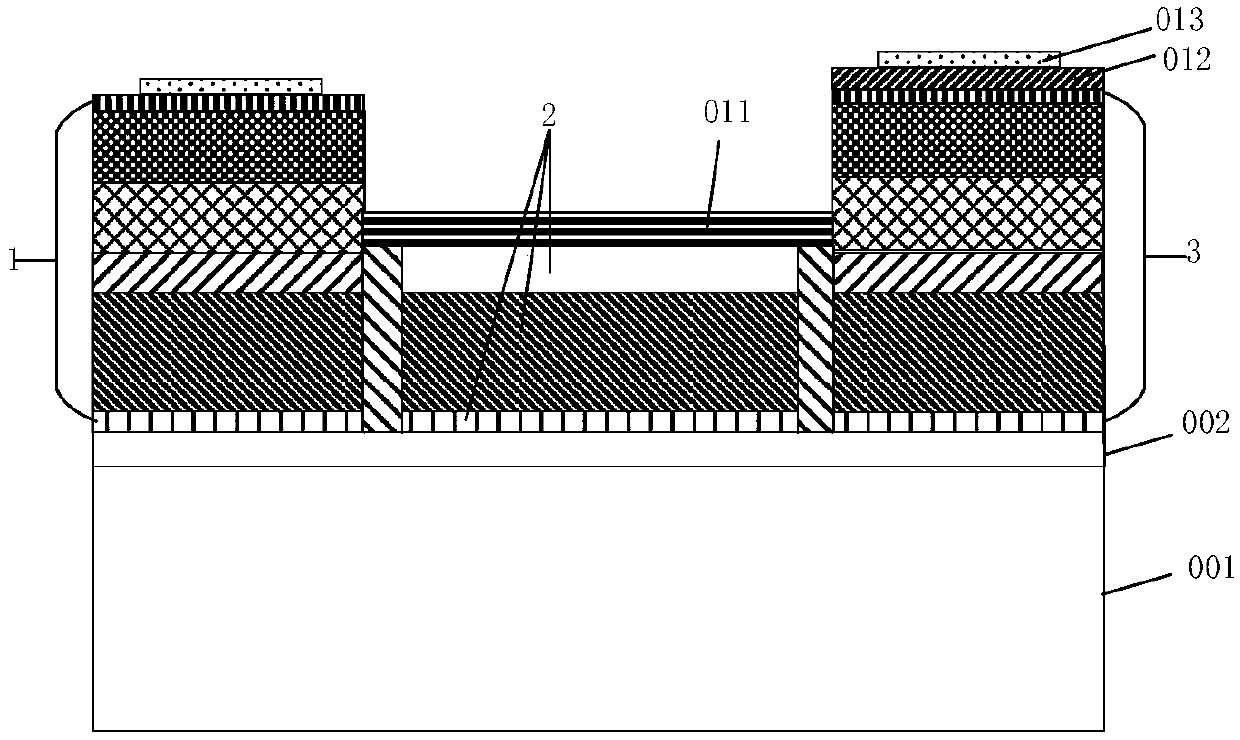
[0047] refer to figure 1 , figure 1 Schematic structure of Si-based modified Ge monolithic same-layer optoelectronic device provided for the present invention Figure 1 , specifically including a substrate 001; a buried layer 002 is disposed on the substrate 001; a light emitter part 1, a waveguide part 2 and a detector part 3 are sequentially arranged on the buried layer 002 from left to right; the light emitter part 1 and the detector part 3 are respectively provided with electrodes 013 .

[0048] Wherein, the substrate 001 is a P-type doped Si substrate 001 with a height of 30-750 nm and a doping concentration of 10 18 cm -3 , the buried layer 002 is a P-type doped Ge layer with a height of 50 nm and a doping concentration of 10 20 cm -3 .

[0049] It should be noted that the light emitter part 1, the waveguide part 2 and the detector part 3 are only arranged in the middle area of ​​the buried layer 002, further, the top of the light emitter part 1 and the detector part...

Embodiment 2

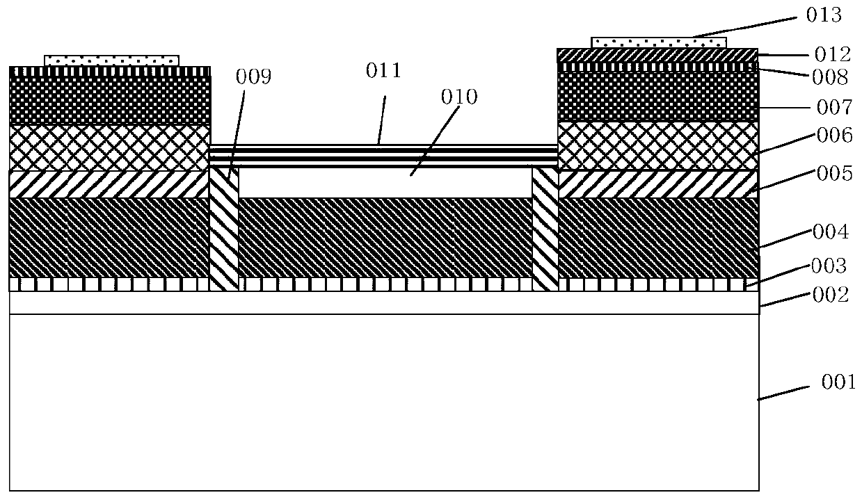
[0079] A method for preparing a Si-based modified Ge monolithic photoelectric device with the same layer provided by the embodiment of the present invention, such as Figure 6a ~ Figure 6n (1) as shown, Figure 6a ~ Figure 6n (1) A schematic diagram of the preparation process of a Si-based modified Ge monolithic same-layer photoelectric integrated device provided by the embodiment of the present invention, the specific steps include:

[0080] S101. Substrate 001 is selected. like Figure 6a As shown, the P-type Si substrate with a height of 30-750nm is selected as the initial material, and the doping concentration is 10 18 cm -3 .

[0081] S102, growing the buried layer 002. like Figure 6b As shown, at a temperature of 330° C., a P-type doped Ge layer with a height of 50 nm is epitaxially grown on the substrate layer 001 by chemical vapor deposition, and the doping concentration is 10 20 cm -3 .

[0082] S103 , growing the first intrinsic Ge layer 003 . like Figur...


PUM

PropertyMeasurementUnit
heightaaaaaaaaaa
heightaaaaaaaaaa
heightaaaaaaaaaa

Abstract

The invention relates to a Si-based modified Ge monolithic same-layer photoelectric device, which comprises a substrate (001), a buried layer (002), a light emitter part (1), a waveguide part (2), a detector part (3) and an electrode (013). Isolation layers (009) are respectively arranged between the waveguide part (2) and the light emitter part (1) and between the waveguide part (2) and the detector part (3); the outer surfaces of the waveguide part (2) and the isolation layer (3) are coated with a first stress film (011); and the outer surface of the detector part (3) and the upper surface of the buried layer (002) are coated with a second stress film (012). According to the technical scheme, the light emitter part (1), the waveguide part (2) and the detector part (3) are integrally arranged on the same substrate (001) and the buried layer (002), so that the device integration degree is high, and the process cost is low; and the waveguide part (2) and the detector part (3) are subjected to energy band modulation through the first stress film (011) and the second stress film (012), so that the forbidden band widths of the light emitter part (1), the waveguide part (2) and the detector part (3) meet the requirements.

Description

technical field [0001] The invention belongs to the field of optoelectronic communication, and in particular relates to a Si-based modified Ge monolithic same-layer optoelectronic device. Background technique [0002] With the continuous development of optical communication technology, the miniaturization and low power consumption of photoelectric signal conversion equipment have become more and more urgent. In the fields of optical devices, electrical devices and optoelectronic integration, III-V semiconductor materials have been widely used, but their incompatibility with the existing Si process, high production cost and long process cycle restrict their further development. development of. [0003] The materials used in photon integrated circuit (PIC) and optielectronics integrated circuit (OEIC) include Si, Ge of group IV, GaAS, InP and ternary and quaternary alloys of group I~V compounds, etc. Semiconductor materials, because silicon has a higher degree of crystal int...

Claims


Application Information

Patent Timeline
Patent Type & Authority Applications(China)
IPC IPC(8): H01L31/153H01L31/173H01L31/18
CPCH01L31/153H01L31/173H01L31/1812Y02P70/50
Inventor 薛磊
Owner XIAN CREATION KEJI CO LTD
Why Eureka
Try Eureka