Lateral double diffused field effect transistor, manufacturing method, chip and circuit

A technology of field effect transistors and lateral double diffusion, which is applied in the direction of circuits, semiconductor/solid-state device manufacturing, electrical components, etc., can solve the problems of driving ability and speed difference, and achieve increased speed, improved carrier mobility, and weakened band The effect of scattering

Active Publication Date: 2022-05-31
BEIJING CHIP IDENTIFICATION TECH CO LTD +1
View PDF16 Cites 0 Cited by
  • Summary
  • Abstract
  • Description
  • Claims
  • Application Information

AI Technical Summary

Problems solved by technology

[0004] Aiming at the technical problem of poor driving capability and speed of lateral double diffused field effect transistors in the prior art, the present invention provides a method for manufacturing a lateral double diffused field effect transistor, a lateral double diffused field effect transistor, a chip and a A kind of circuit, the lateral double-diffusion field effect transistor prepared by this method can improve the mobility of carriers in the channel, and improve the driving ability and speed of the transistor

Method used


Image

  • Lateral double diffused field effect transistor, manufacturing method, chip and circuit
  • Lateral double diffused field effect transistor, manufacturing method, chip and circuit
  • Lateral double diffused field effect transistor, manufacturing method, chip and circuit

Examples


Embodiment Construction

[0031] The specific implementation of the embodiments of the present invention will be described in detail below in conjunction with the accompanying drawings. It should be understood that this

[0034] The present invention will be described in detail below with reference to the accompanying drawings and in conjunction with the embodiments.

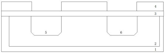
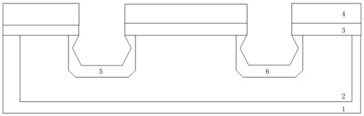
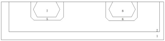
[0038] A first drain 10 is formed in the first tensile strain region 7, a second drain 11 is formed in the second tensile strain region 8, and a P-type body is formed.

[0039] Through the lateral double diffusion field effect transistor of the embodiment of the present invention, a strained material is embedded in the drift region to form

[0040] Further, the first tensile strain region 7 and the second tensile strain region 8 are hexagonal structures.

[0042] Further, the first tensile strain region 7 and the second tensile strain region 8 include silicon carbide.

[0044] Further, the first tensile strain region 7 and the second tensile...


PUM


Abstract

The invention provides a lateral double-diffused field effect transistor, a manufacturing method, a chip and a circuit. The transistor includes: a substrate with a high-voltage N-type well; a first N-type drift region, a P-type body region and a second The N-type drift region is formed in the high-voltage N-type well; the first strained region is formed in the first N-type drift region; the second strained region is formed in the second N-type drift region; the first drain is formed in the second N-type drift region. One strain region; the second drain, formed in the second strain region; the first source and the second source, formed in the P-type body region; the substrate electrode, formed in the first source and the second source between; the first gate, formed on the upper surface of the first N-type drift region and the P-type body region; the second gate, formed on the upper surface of the P-type body region and the second N-type drift region, and the second gate A space is formed between the electrode and the first grid. The transistor provided by the invention can improve the mobility of carriers in the channel, and improve the driving ability and speed of the transistor.

Description

Lateral double diffusion field effect transistor, fabrication method, chip and circuit technical field The present invention relates to semiconductor technology field, particularly, relate to a kind of lateral double diffusion field effect transistor fabrication method Method, a lateral double diffusion field effect transistor, a chip and a circuit. Background technique Lateral Double Diffused Field Effect Transistor (Lateral Double-Diffused MOSFET, LDMOS) is used as a kind of Lateral power devices, whose electrodes are all located on the surface of the device, are easily connected to low-voltage signal circuits and other The monolithic integration of the device also has the advantages of high withstand voltage, large gain, good linearity, high efficiency, and good broadband matching performance. Nowadays, it has been widely used in power integrated circuits, especially low-power and high-frequency circuits. In the prior art, the lateral double diffusion field effe...

Claims


Application Information

Patent Timeline
Patent Type & Authority Patents(China)
IPC IPC(8): H01L29/06H01L29/78H01L21/336
Inventor 余山赵东艳王于波陈燕宁付振刘芳王凯吴波邓永峰刘倩倩郁文
Owner BEIJING CHIP IDENTIFICATION TECH CO LTD
Why Eureka
Try Eureka