Group-III nitride p-type ohmic electrode structure with low contact resistance

A technology of low contact resistance and electrode structure, applied in the direction of circuits, electrical components, laser components, etc., can solve problems such as low solid solubility, limited tunneling effect, and limited concentration, achieve high tunneling probability characteristics, and improve ohm Contact characteristics and the effect of reducing contact resistivity

Active Publication Date: 2020-12-22
SUN YAT SEN UNIV
View PDF3 Cites 0 Cited by
  • Summary
  • Abstract
  • Description
  • Claims
  • Application Information

AI Technical Summary

Problems solved by technology

However, due to the high ionization energy of acceptors in wide-bandgap semiconductors (the ionization energy of Mg acceptor impurities in GaN is 150-180meV, which is much higher than the thermal energy of 26meV at room temperature), the ionization rate at room temperature is very low. Low, it is difficult to form an effective number of ions, resulting in limited tunneling; at the same time, due to the low solid solubility of Mg in III-nitride materials, the concentration of heavy doping is limited, and excessive heavy doping will not only The generation of derivative compounds and complexes of Mg will also lead to deterioration of crystal quality and increase of surface roughness, which is not conducive to device fabrication
These factors all hinder the formation of good p-type ohmic contact of GaN-based materials, so that the p-type ohmic contact resistance needs to be further reduced

Method used


Image

  • Group-III nitride p-type ohmic electrode structure with low contact resistance
  • Group-III nitride p-type ohmic electrode structure with low contact resistance
  • Group-III nitride p-type ohmic electrode structure with low contact resistance

Examples


Embodiment Construction

[0022] The present invention will be described in further detail below in conjunction with accompanying drawing:

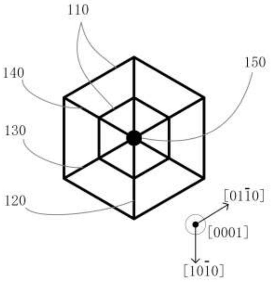
[0023] see figure 1 As shown, as the first embodiment of the present invention, the electrode structure is a regular hexagonal spider web shape, including two concentric regular hexagonal line bodies 110, connecting three pairs of opposite corners of the regular hexagonal line bodies The three positive diagonal lines (120, 130, 140), the welding wire electrode part 150 located at the geometric center of the electrode structure or the intersection of any electrode pattern line body, there are two groups of the three groups of opposite sides of the regular hexagonal line body They are respectively consistent with the first crystal orientation and the second crystal orientation of the III-group nitride, and the remaining group is consistent with the equivalent crystal orientation of the first crystal orientation and the second crystal orientation of the III-group ni...


PUM


Abstract

The invention relates to the technical field of semiconductor devices, in particular to an III-nitrides p-type ohmic electrode structure with low contact resistance. The direction of an electrode pattern line body of the electrode structure is consistent with a first crystal orientation or a second crystal orientation and an equivalent crystal orientation of the first crystal orientation and the second crystal orientation of III-nitrides; after clockwise rotating for 120 degrees, the first crystal orientation is parallel to the second crystal orientation; and a bonding wire electrode part of the electrode structure is located at the geometric center of the electrode structure or at a cross point of any electrode pattern line body. The electrode structure in the invention aims to obtain good ohmic contact characteristic on the p-type III-nitrides material; the high tunneling probability characteristic of a hole in the crystal orientation and the equivalent crystal orientation of the III-nitrides material is effectively utilized by the proposed electrode structure along the crystal orientation, thereby reducing electrical resistivity of ohmic contact.

Description

technical field [0001] The invention relates to the technical field of semiconductor devices, in particular to a group III nitride p-type ohmic electrode structure with low contact resistance. Background technique [0002] Compound semiconductor gallium nitride (GaN)-based materials have excellent chemical and chemical properties such as wide direct band gap, strong atomic bond, high thermal conductivity, good chemical stability, strong radiation resistance, and fast electron saturation migration speed. physical properties. In particular, by adjusting the composition of the GaN-based material ternary compounds AlGaN, AlInN and InGaN, and the quaternary compound AlInGaN, the band gap of the material can be changed, the energy band can be tailored, and the corresponding wavelength of the band gap can be changed from infrared to deep ultraviolet. continuous change. The advantages of these material properties make the III-nitrides represented by GaN have received extensive att...

Claims


Application Information

Patent Timeline
Patent Type & Authority Patents(China)
IPC IPC(8): H01L29/45H01L31/0224H01L33/36H01S5/042
CPCH01L29/452H01L31/022408H01L33/36H01S5/0425
Inventor 江灏邱新嘉
Owner SUN YAT SEN UNIV
Why Eureka
Try Eureka