
GALLIUM NITRIDE ON 3C-SiC COMPOSITE WAFER

a gallium nitride and composite wafer technology, applied in the direction of basic electric elements, semiconductor devices, electric devices, etc., can solve the problem of presenting the same stress problems

Active Publication Date: 2016-08-25
ANVIL SEMICON
View PDF0 Cites 14 Cited by
  • Summary
  • Abstract
  • Description
  • Claims
  • Application Information

AI Technical Summary

Benefits of technology

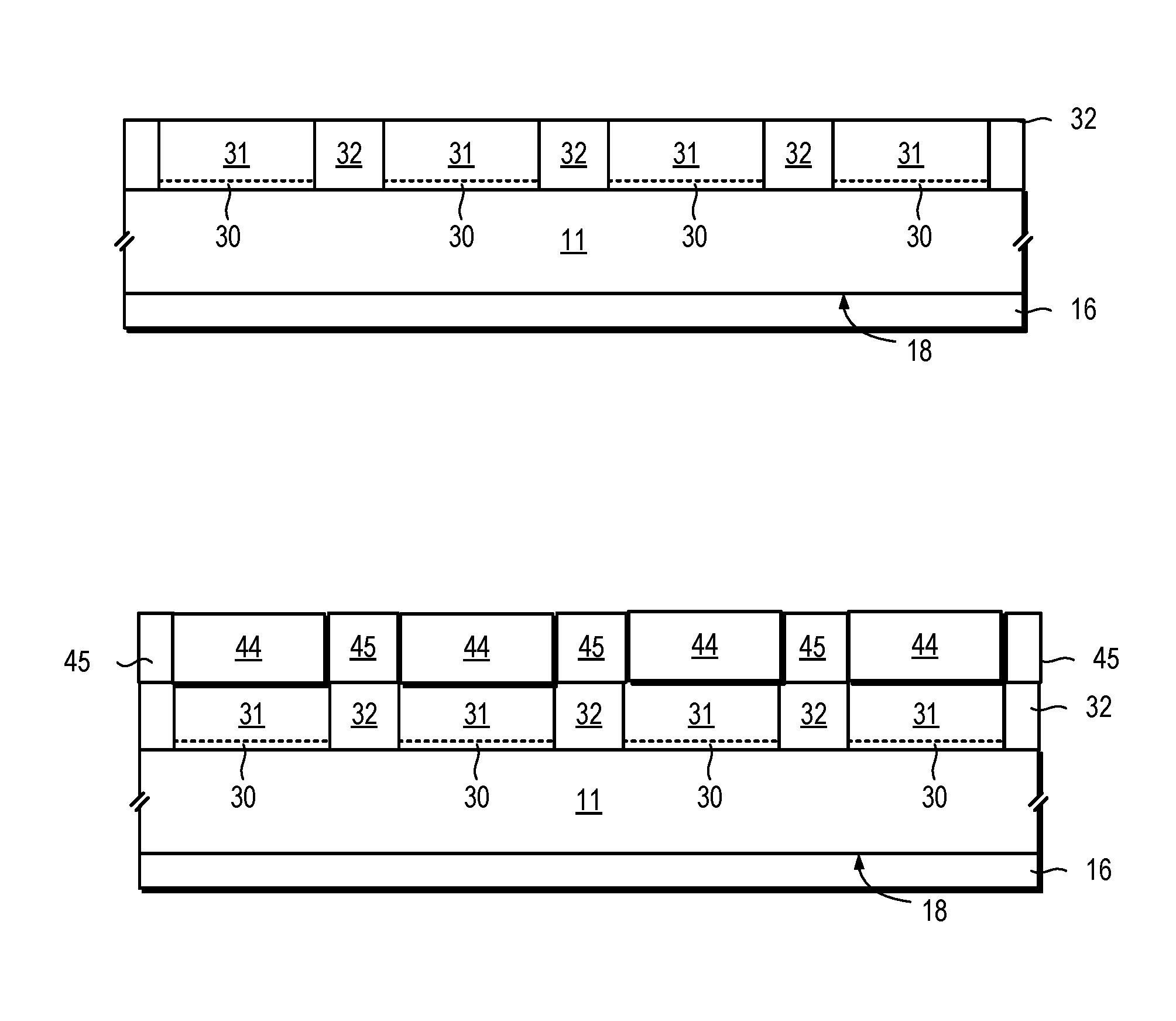
The patent describes a method for reducing stress and bowing in a wafer that includes multiple layers of gallium nitride. Segmented growth of the layers is advantageous in reducing the negative effects of stress across the entire wafer. Additionally, cutting the initial mask in a way that reflects the growth of the underlying layers can help to control stress locally in individual cells. Overall, this method improves the quality and efficiency of manufacturing of gallium nitride wafers.

Problems solved by technology

However, the heterogrowth process for forming GaN on Si wafer presents the same stress problems that have been faced with silicon carbide (SiC) on Si.

Method used


Image

  • GALLIUM NITRIDE ON 3C-SiC COMPOSITE WAFER
  • GALLIUM NITRIDE ON 3C-SiC COMPOSITE WAFER
  • GALLIUM NITRIDE ON 3C-SiC COMPOSITE WAFER

Examples


Embodiment Construction

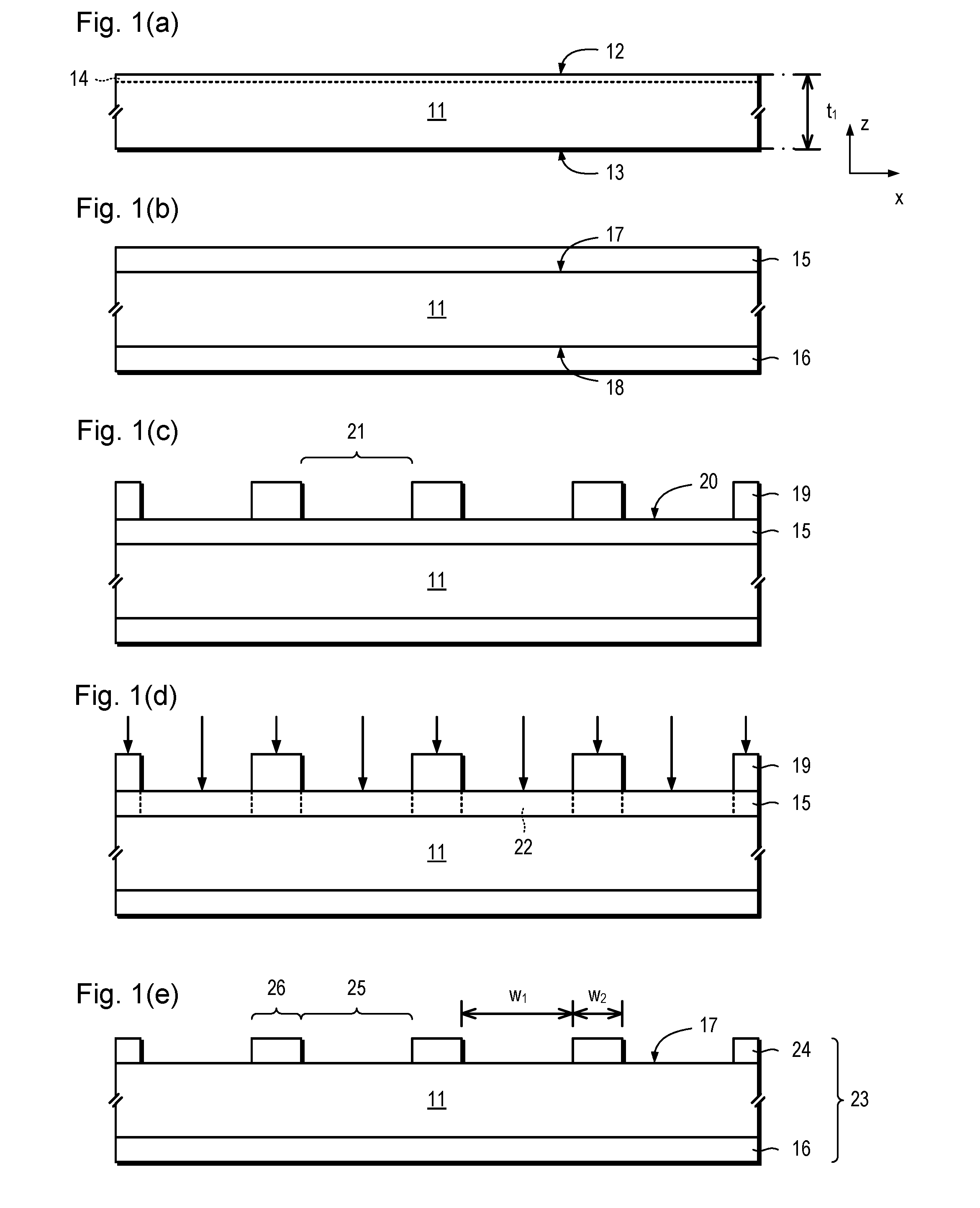
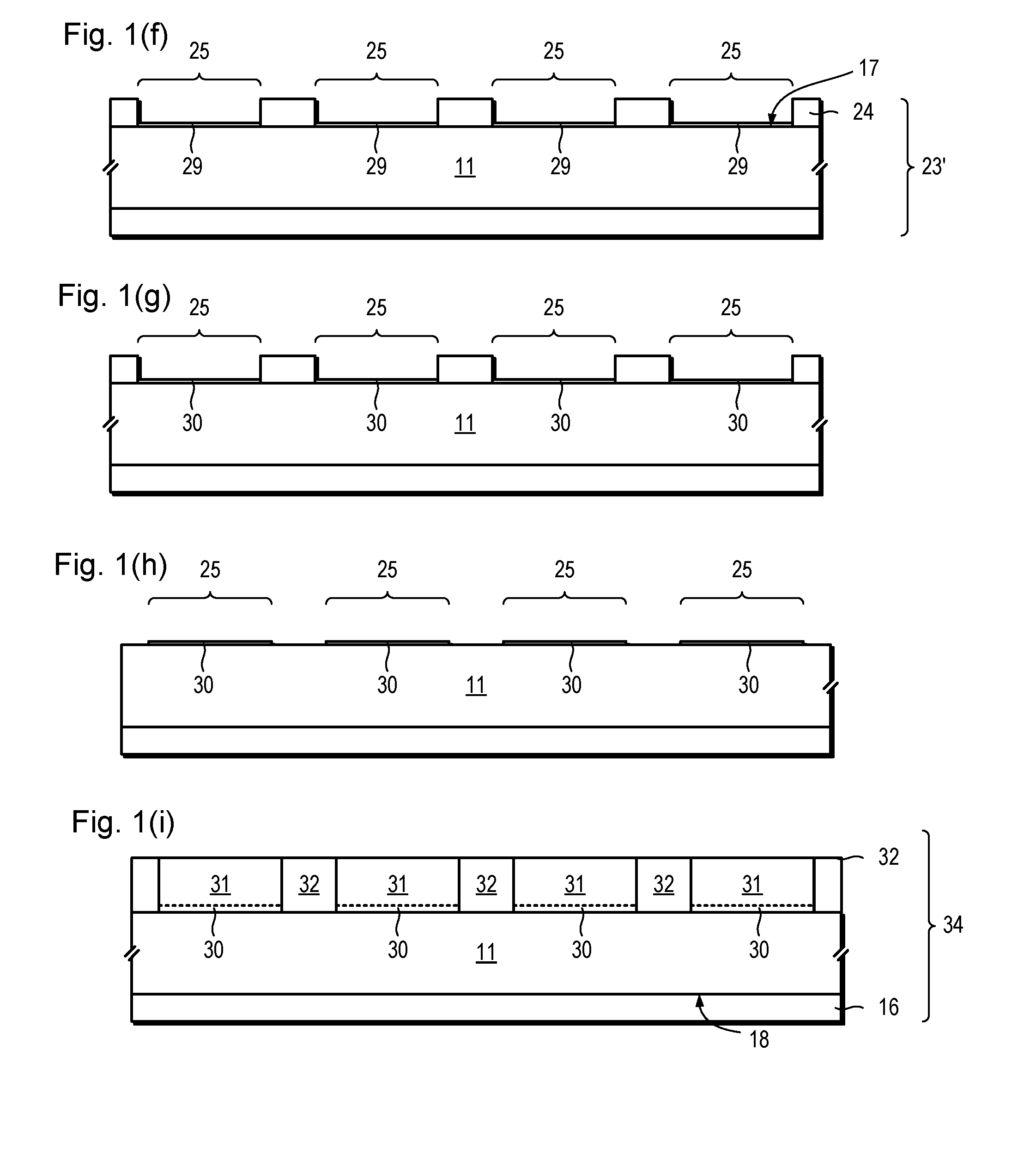
[0054]Referring to FIGS. 1a to 1i, an embodiment of a method of fabricating silicon carbide semiconductor devices which includes silicon carbide / silicon heteroepitaxy is described.

[0055]FIG. 1a shows a monocrystalline silicon wafer 11 at a room temperature.

[0056]The silicon wafer 11 may have an off-axis, [111] crystal orientation and may be polished on one or both sides 12, 13. The sides 12, 13 may also be referred to as “surfaces” or “faces”. Other crystal orientations may be used, such as [100] on or off axis. The silicon wafer 11 has a thickness, t1, and a diameter, d1 (not shown). In this example, t1=750 μm and d1=100 mm. In an alternative example, t1=about 750 μm to 1000 μm and d1=150 mm The silicon wafer 11 has a wafer bow less than 25 μm and so can be considered to have substantially no bow.

[0057]The silicon wafer 11 serves as a crystal matrix on which a layer of monocrystalline three-step cubic silicon carbide can be epitaxially grown on a first side 12 of the wafer 11 (here...


PUM

PropertyMeasurementUnit
temperatureaaaaaaaaaa
thicknessaaaaaaaaaa

Abstract

We disclose a semiconductor structure comprising a monocrystalline silicon wafer; spaced apart monocrystalline silicon carbide layers disposed directly on the silicon wafer; amorphous and / or polycrystalline silicon carbide layers disposed directly on the silicon wafer between the monocrystalline silicon carbide layers; first gallium nitride layers disposed on the monocrystalline silicon carbide layers; and second gallium nitride layers disposed on the amorphous and / or polycrystalline silicon carbide layers.

Description

FIELD OF THE INVENTION[0001]This invention relates to growing cubic gallium nitride (GaN) on a 3-step silicon carbide (3C—SiC) composite wafer, particularly but not exclusively, relates to reducing material stress in cubic GaN formed on SiC composite wafer and to bow reduction in the wafer.BACKGROUND TO THE INVENTION[0002]There is a considerable interest around the world in growing GaN on silicon (Si) wafer for light emitting diodes (LEDs) and power devices. However, the heterogrowth process for forming GaN on Si wafer presents the same stress problems that have been faced with silicon carbide (SiC) on Si.[0003]It has been demonstrated by the “Anvil Grid” process that the use of a silicon dioxide (SiO2) grid between die which is destroyed during the temperature ramp to the growth temperature (Carbonisation) produces a growth in these grid regions of polycrystalline SiC. This produces a low stress region between the monocrystalline SiC die which inevitably contain a tensile stress. I...

Claims


Application Information

Patent Timeline
Patent Type & Authority Applications(United States)
IPC IPC(8): H01L33/12H01L33/00H01L33/32H01L21/02
CPCH01L33/12H01L21/02381H01L21/02447H01L21/02513H01L33/32H01L21/0259H01L21/0262H01L33/007H01L33/0095H01L21/0254H01L21/02433
Inventor WARD, PETER
Owner ANVIL SEMICON
Learn More