Method of integrating inorganic light emitting diode with oxide thin film transistor for display applications

a technology of light emitting diodes and thin film transistors, applied in semiconductor devices, instruments, electrical devices, etc., can solve the problems of inorganic led devices that lack very high brightness, limited lifetime, and limitations in fabrication technology, and achieve high brightness, cure deficiencies, and high contrast

Active Publication Date: 2016-10-06
EMAGIN CORP
View PDF5 Cites 63 Cited by
  • Summary
  • Abstract
  • Description
  • Claims
  • Application Information

AI Technical Summary

Benefits of technology

[0014]The present invention cures the deficiencies in the prior art by providing a method for integrating inorganic LED with oxide TFT for display applications. An oxide TFT is a kind of field-effect transistor made by depositing thin forms of semiconductor active layer as well as the dielectric layer and metallic contacts over a supporting substrate. In oxide TFT the material of the electron channel is oxide. The present method involves the deposition of oxide TFT layers onto a previously fabricated GaN type LED substrate. By incorporating an oxide TFT with a III-V type (e.g. GaN) LED array an active matrix display is realized with extremely high brightness, high contrast, and extended lifetime.
[0019]In accordance with another illustrative embodiment of the present invention, a method of fabricating a light emitting device is disclosed. The steps include forming a compound stacked semiconductor structure over a substrate, wherein the semiconductor structure includes an n-type type semiconductive layer formed on the substrate comprising a material selected from the group consisting of III-V and II-VI compounds, a p-type semiconductive layer overlying the n-type semiconductive layer comprising a material selected from the group consisting of III-V and IV-VI compounds, electrically coupling a first electrode with the n-type semiconductive layer, and electrically coupling a second electrode with the p-type semiconductive layer. Then, forming an insulating layer comprising dielectric material over the semiconductor structure in a manner which does not cause significant damage to the structure. Then, forming conductive vias through the insulating layer, and forming a metal oxide thin film transistor backplane over the insulating layer and conductive vias in a manner which does not cause significant damage to the semiconductor structure.

Problems solved by technology

However, OLEDs devices lack very high brightness and are limited in lifetime.
In addition, the lifetime of inorganic LED devices is extremely long.
The notable drawbacks of inorganic LEDs include limitations in fabrication technology and the high cost of fabrication.
Until now, the main problem with fabricating inorganic LED technology for display applications was the drive circuit.
Therefore, a display device using just GaN had not been feasible.
There have been many attempts to combine the Si technology for driving the GaN LEDs to fabricate displays, however, they have been largely unsuccessful.
As such, inorganic LEDs are still not a part of the display industry.

Method used


Image

  • Method of integrating inorganic light emitting diode with oxide thin film transistor for display applications
  • Method of integrating inorganic light emitting diode with oxide thin film transistor for display applications
  • Method of integrating inorganic light emitting diode with oxide thin film transistor for display applications

Examples


Embodiment Construction

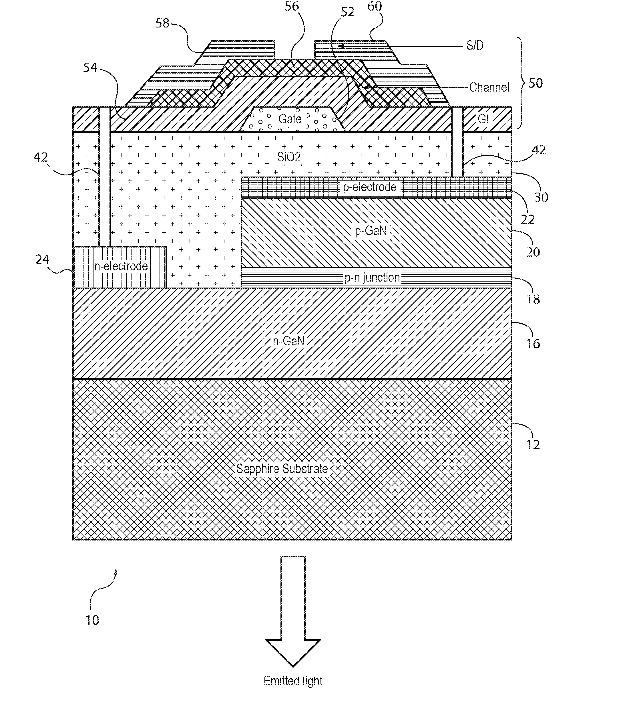
[0032]The present invention is directed to methods of integrating light emitting diodes (LEDs) with thin film transistors (TFTs) for display applications. In particular, the present invention utilizes III-V or II-VI group compound semiconductor materials to form LED devices. These materials require temperatures greater than 700C for processing. It should be noted that the materials and processes described herein are for illustrative purposes and the present invention is not limited to the specific LED devices or TFT configurations described.

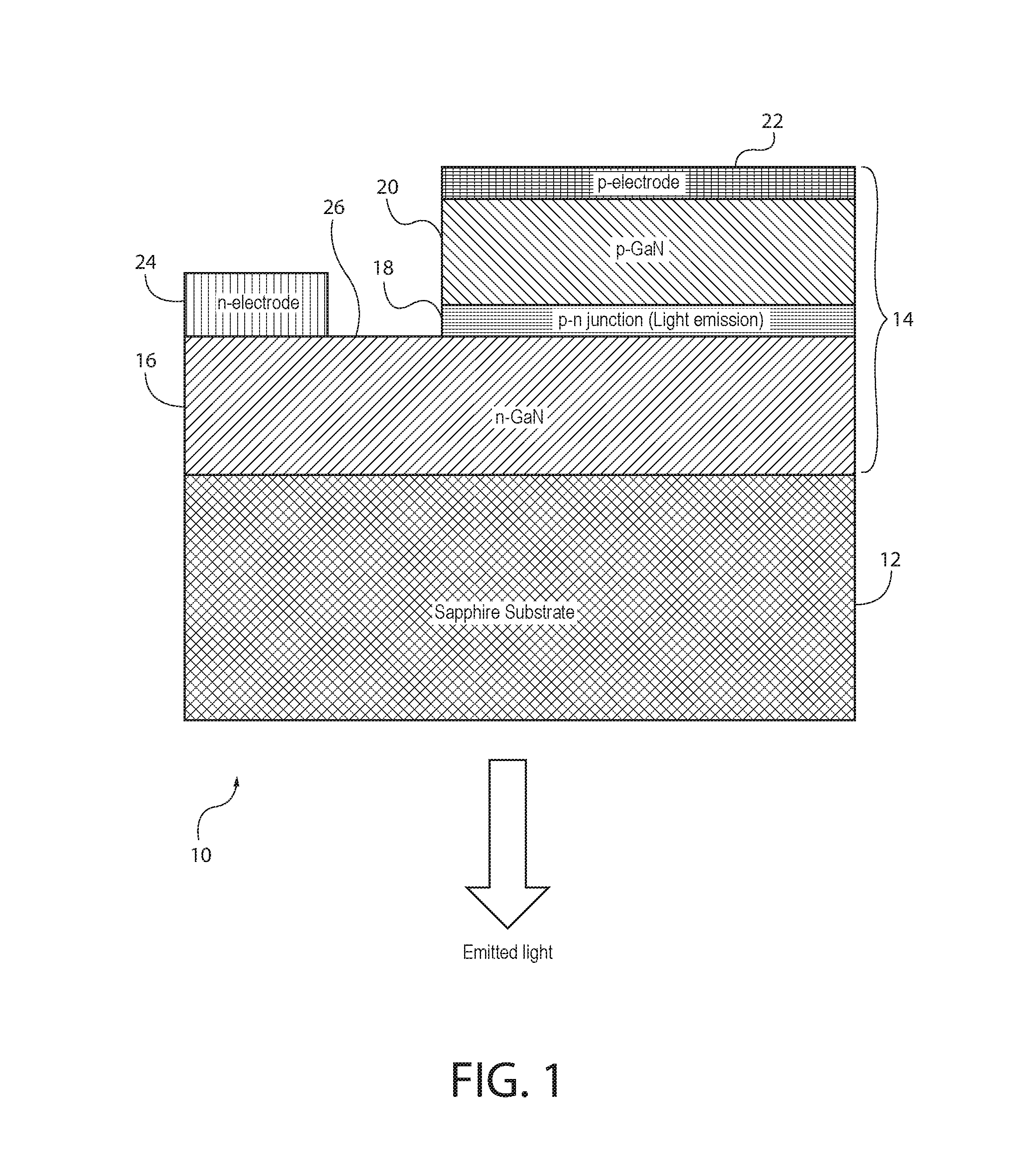
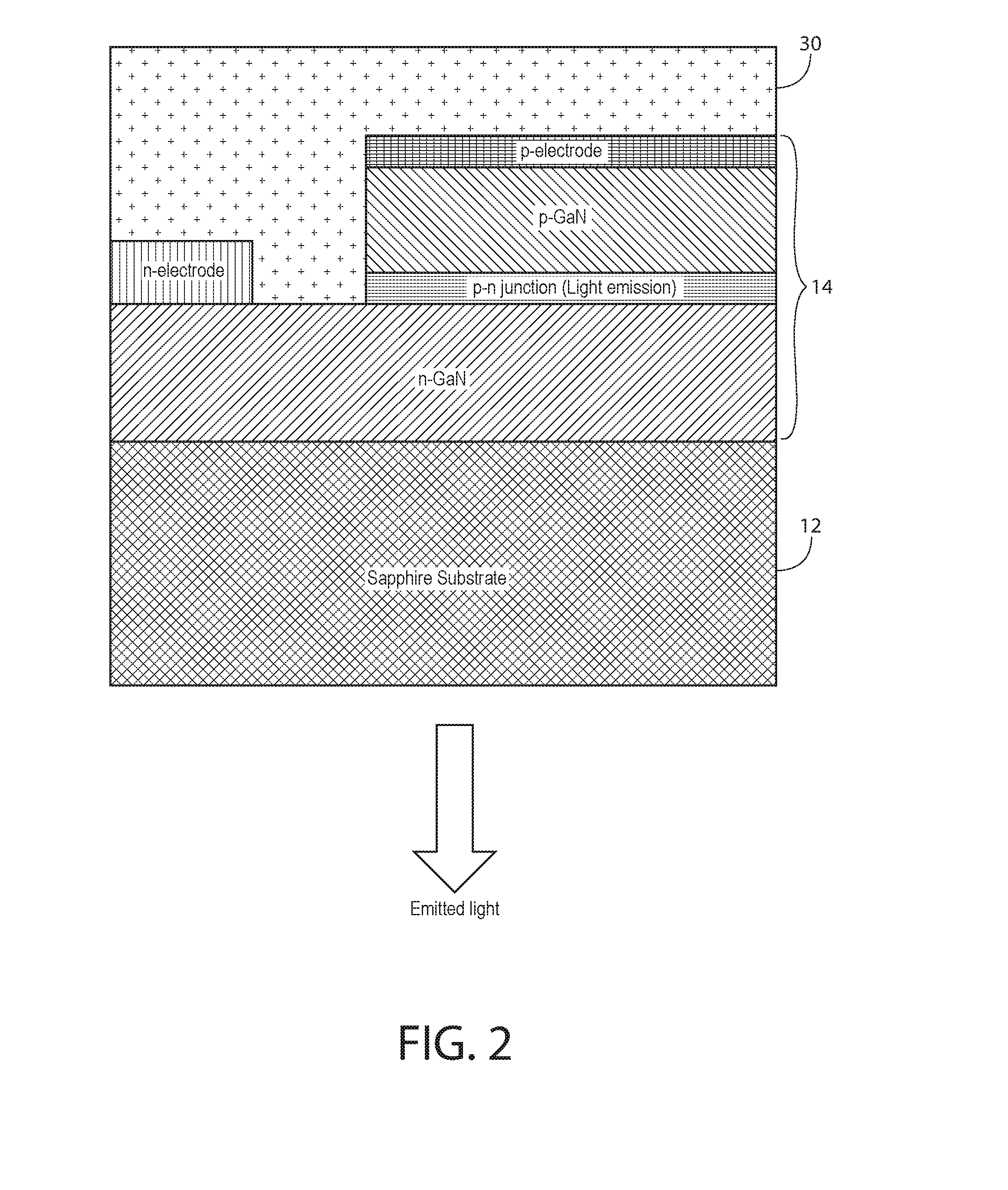
[0033]FIGS. 1-4 illustrate the sequence of steps used in fabricating a TFT array on a LED array, having a plurality of sub-pixels, according to the present method. FIG. 1 illustrates an LED wafer 10 according to an illustrative embodiment of the present invention. The LED wafer 10 includes a stacked structure 14 composed on a transparent substrate 12. The structure 14 includes a first type semiconductive layer 16 positioned on the substrate 12, a...


PUM


Abstract

A method of fabricating an active matrix display is disclosed in which one or more oxide thin film transistors is monolithically integrated with an inorganic light emitting diode structure. The method comprises forming an array of inorganic light emitting diodes over a substrate defining a plurality of sub-pixels, depositing an insulating layer over the inorganic LED array, forming conductive vias through the insulating layer, one via for each LED in the LED array, and forming a metal oxide thin film transistor backplane, including an array of pixel driver circuits, over the dielectric layer and conductive vias, wherein one driver circuit electrically controls each sub-pixel through the dielectric layer.

Description

CROSS-REFERENCE TO RELATED APPLICATION[0001]This application claims priority to provisional patent application Ser. No. 62 / 139,888 filed in the United States Patent and Trademark Office on Mar. 30, 2015, the entire disclosure and drawings of which are incorporated in their entirety by reference herein.FIELD OF THE INVENTION[0002]The present invention relates generally to methods of integrating light emitting diodes (LEDs) with thin film transistors (TFTs) for display applications, and more particularly to a method of monolithically integrating inorganic LEDs with metal oxide TFTs.BACKGROUND OF THE INVENTION[0003]Two kinds of light emitting diodes (LED) exist today. One is based on organic materials (OLED), while the other one is based on inorganic materials. Both kinds of LEDs essentially work on similar principles wherein positive and negative charge carriers are injected into a semiconducting material and light emission occurs when the charge carriers recombine in the light emissi...

Claims


Application Information

Patent Timeline
Patent Type & Authority Applications(United States)
IPC IPC(8): H01L25/16H01L29/66H01L29/786H01L33/00H01L33/32H01L33/28
CPCH01L25/167H01L33/32H01L33/28H01L29/66969H01L33/007H01L33/0087H01L29/7869G02F1/1368H01L25/0756
Inventor GHOSH, AMALKUMAR P.
Owner EMAGIN CORP
Why Eureka
Try Eureka