Semiconductor device with thin-film resistor

Active Publication Date: 2016-10-13
GLOBALFOUNDRIES US INC
View PDF2 Cites 0 Cited by
  • Summary
  • Abstract
  • Description
  • Claims
  • Application Information

AI Technical Summary

Benefits of technology

The present invention improves the manufacturing of semiconductor devices, particularly those with resistor structures. The invention involves adding a thin layer of metal-containing material (often titanium nitride) between the resistor and the first semiconductor layer. This layer acts as a barrier to prevent current leakage and improves the reliability of the overall production process. The method includes steps to form the metal-containing layer, a first semiconductor layer, and a contact to the metal-containing layer. The use of a silicon-based semiconductor layer on an SOI wafer can also improve reliability.

Problems solved by technology

In principle, the known polysilicon resistors have disadvantages due to local density variations and doping material inhomogeneities.
Such manufacturing variations become of course increasingly unfavorable with a growing miniaturization of the ICs.
A reliable setting of clearly defined resistance values is therefore more complicated.
However, during etching of the apertures for the contacts 7 in the interlayer dielectric 8, there is the risk of etching through the NiSi layer 6.
This risk of etching through, which is connected to an undesired changed resistor behavior, is another disadvantage of the manufacturing process of integrated polysilicon resistors of the state of the art.

Method used


Image

  • Semiconductor device with thin-film resistor
  • Semiconductor device with thin-film resistor
  • Semiconductor device with thin-film resistor

Examples


Embodiment Construction

[0020]Although the present invention is described with reference to the embodiments as they are illustrated in the following detailed descriptions as well as in the drawings, it should be taken into account that the following detailed description as well as the drawings do not intend to limit the present invention to the specific illustrative embodiments, but that the described illustrative embodiments rather show the diverse aspects of the present invention whose scope of protection, in contrast, is defined exclusively and in an exemplary way by the enclosed patent claims.

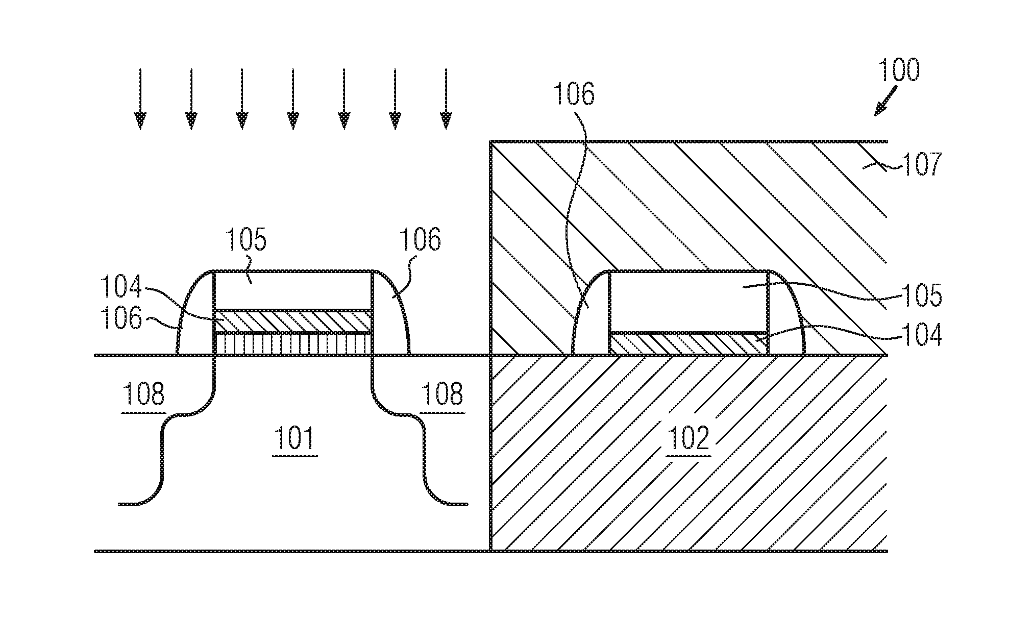
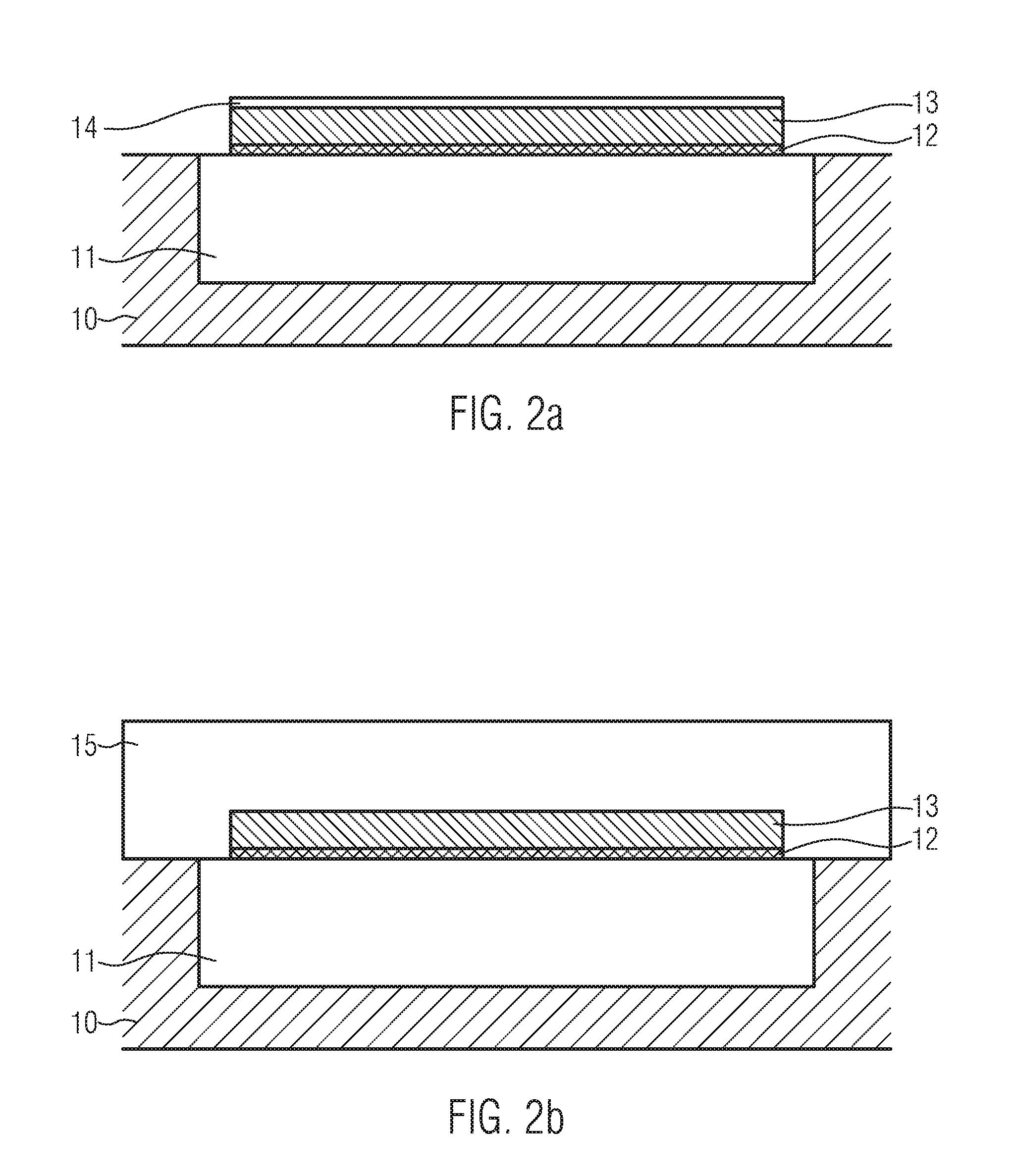
[0021]The present invention generally relates to semiconductor devices and processes for their production, whereby resistor structures with a high degree of compatibility with conventional SOI manufacturing processes are produced. The resistor structures are formed of a thin metal-containing layer that can also be used for the formation of gate electrodes of TFTs as part of the general manufacturing process.

[0022]...


PUM


Abstract

A semiconductor device with a metal-containing layer, a first semiconductor layer, that is formed on top of the metal-containing layer, and a resistor that is formed in the metal-containing layer and that is contacted through the first semiconductor layer is provided. Furthermore, a method of manufacturing a semiconductor device is provided, wherein the method comprises manufacturing of a resistor with the following steps: formation of a metal-containing layer over a wafer, particularly a SOI wafer, formation of a first semiconductor layer on top of the metal-containing layer and formation of a contact through the semiconductor layer to the metal-containing layer.

Description

FIELD OF THE PRESENT INVENTION[0001]The present invention generally relates to the field of manufacturing of integrated circuits and relates particularly to resistors that are to be installed in complex integrated circuits.DESCRIPTION OF THE STATE OF THE ART[0002]In modern integrated circuits, a very large number of individual switching elements such as field effect transistors in the form of CMOS, NMOS, PMOS elements, resistors, capacitors and the like is produced on an individual chip area. Typically, the structural sizes of these circuit elements are constantly reduced with the integration of each new circuit generation in order to provide the latest available circuits with an improved performance with regard to speed and / or power input. A reduction of the size of the transistors is an important aspect for the further improvements of the device performance in complex integrated circuits such as CPUS. The reduction of the size typically comes with an increase of the switching spee...

Claims


Application Information

Patent Timeline
IPC IPC(8): H01L27/12H01L29/786H01L23/538H01L21/8258H01L21/768H01L21/762H01L29/66H01L49/02H01L29/06
CPCH01L27/1207H01L28/20H01L29/78603H01L29/78675H01L23/5384H01L21/8258H01L29/0649H01L21/76898H01L21/762H01L29/66757H01L23/5386H01L27/0629H01L28/24H01L21/76805H01L21/84
Inventor MOLL, HANS-PETERSIDELNICOV, ANDREIWIATR, MACIEJ
Owner GLOBALFOUNDRIES US INC
Why Eureka
Try Eureka