Ac-dc converter

a converter and dc technology, applied in the direction of dc-dc conversion, power conversion systems, instruments, etc., can solve the problems of limited examples of such circuits and complex control operations, and achieve the effects of low loss, low resistance voltage, and high device efficiency

Active Publication Date: 2016-10-13
FUJI ELECTRIC CO LTD
View PDF4 Cites 7 Cited by
  • Summary
  • Abstract
  • Description
  • Claims
  • Application Information

AI Technical Summary

Benefits of technology

[0056]According to at least some aspects of the present invention, it is possible to configure an AC-DC converter capable of accommodating a high AC voltage input without using semiconductor devices with a high withstand voltage. In other words, by using semiconductor devices having a low withstand voltage and producing a low level of loss, it is possible to achieve higher efficiency in the device as a whole, and to reduce the size and cost thereof by selecting appropriate devices.
[0057]Additionally, when staggering the switching timing of the plurality of switching units connected in s

Problems solved by technology

However, the greater the voltage levels, the more complex the control operation becom

Method used


Image

  • Ac-dc converter
  • Ac-dc converter
  • Ac-dc converter

Examples


embodiment 1

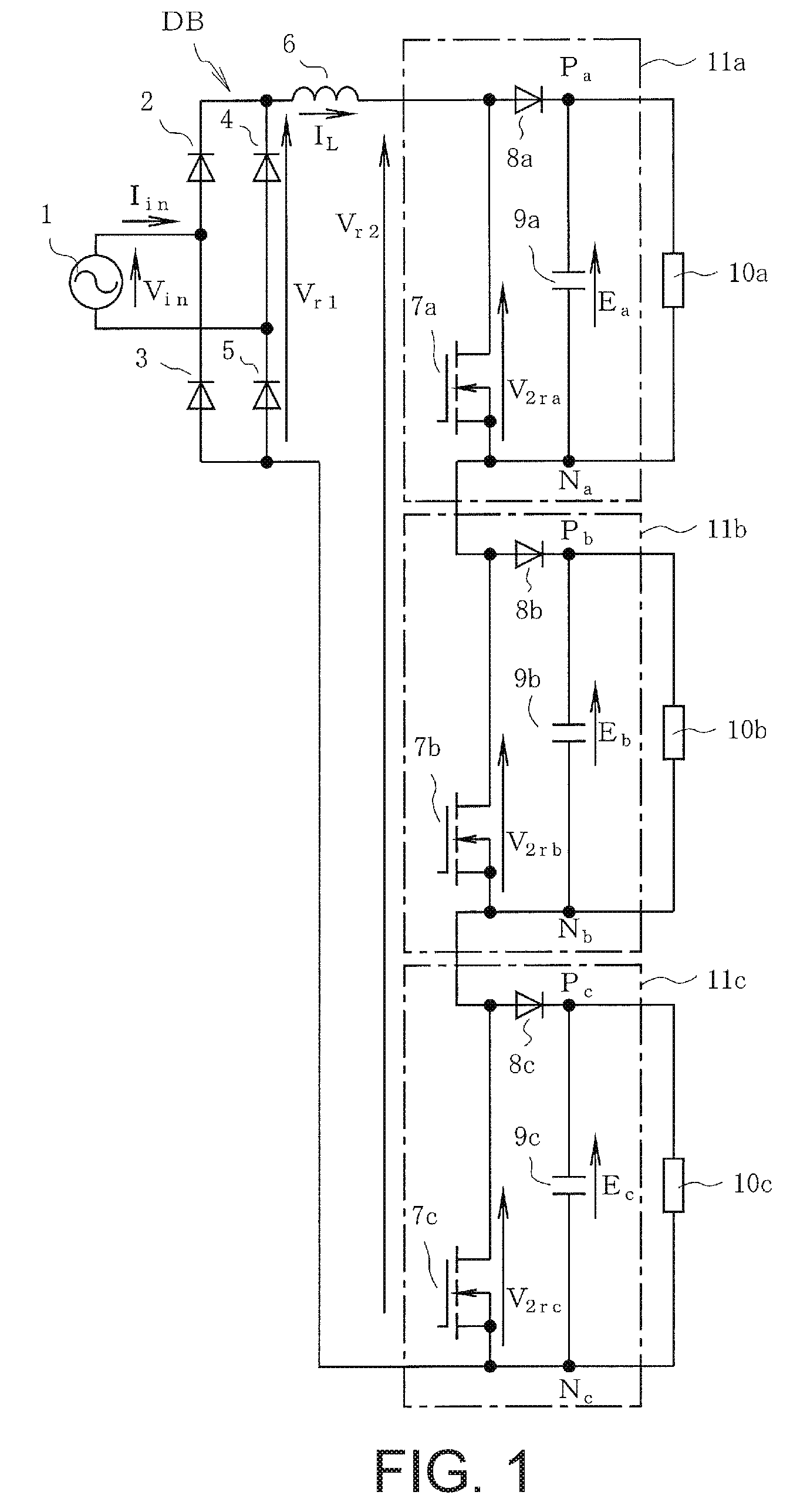
[0074]FIG. 1 is a circuit diagram showing Embodiment 1 of the present invention 1. In FIG. 1, those portions having functions identical to those of FIGS. 10 and 13 are given identical reference characters.

[0075]In FIG. 1, a rectifier circuit DB constituted by diodes 2 to 45 are connected to both ends of an AC power source 1 in a manner similar to the description above. One end of an inductor 6 is connected to a positive-side output terminal of the rectifier circuit DB. Between the other end of the inductor 6 and a negative-side output terminal of the rectifier circuit DB, semiconductor switching devices 7a, 7b, and 7c are connected in series. Other than the MOSFETs shown in the diagram, IGBTs or BJTs may also be used as the switching devices 7a, 7b, and 7c.

[0076]Between the drain and source terminals of the switching device 7a, a diode 8a and a capacitor 9a are connected in series, and a load 10a is connected to the capacitor 9a in parallel. Additionally, between the drain and sour...

embodiment 2

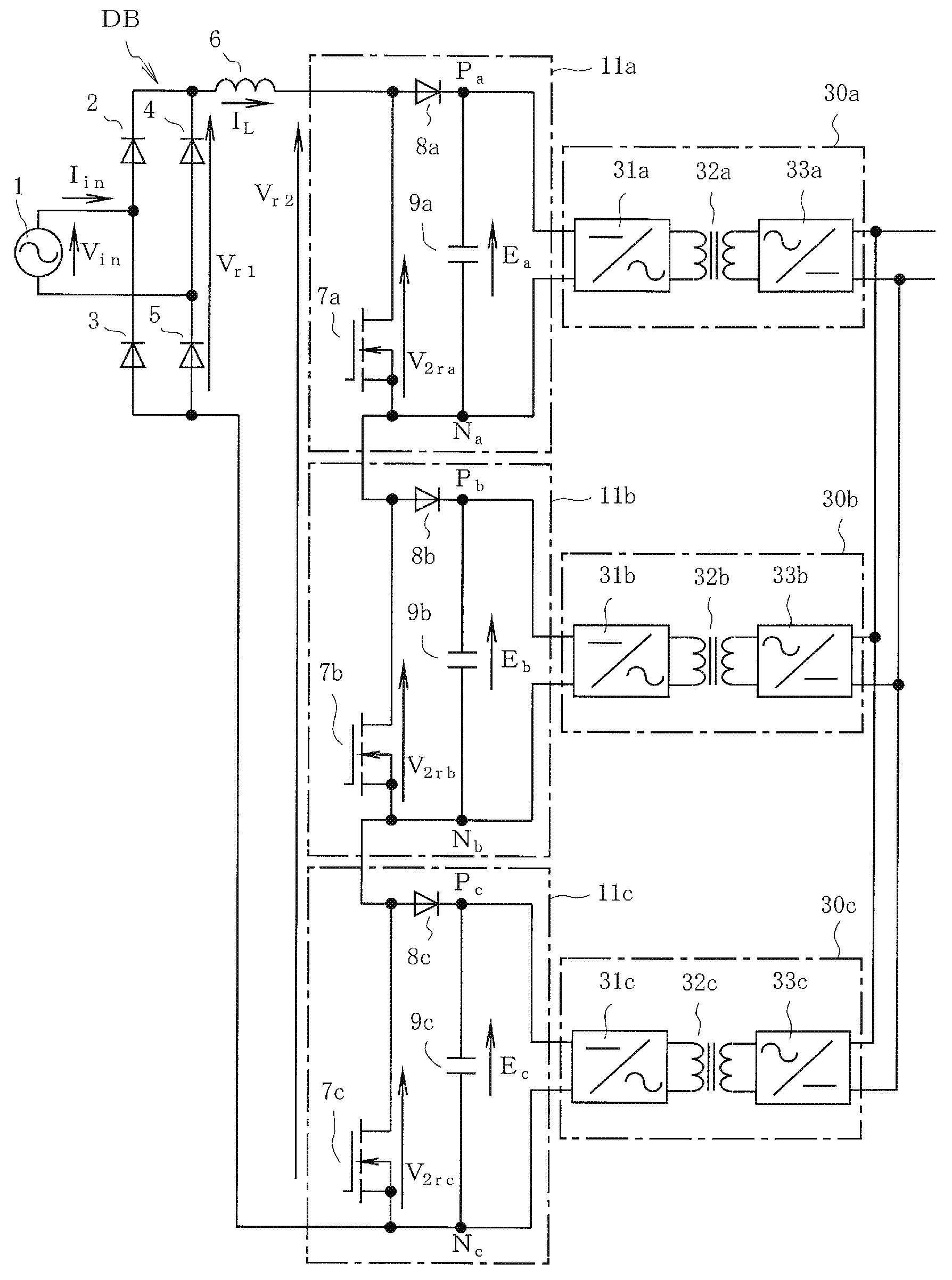
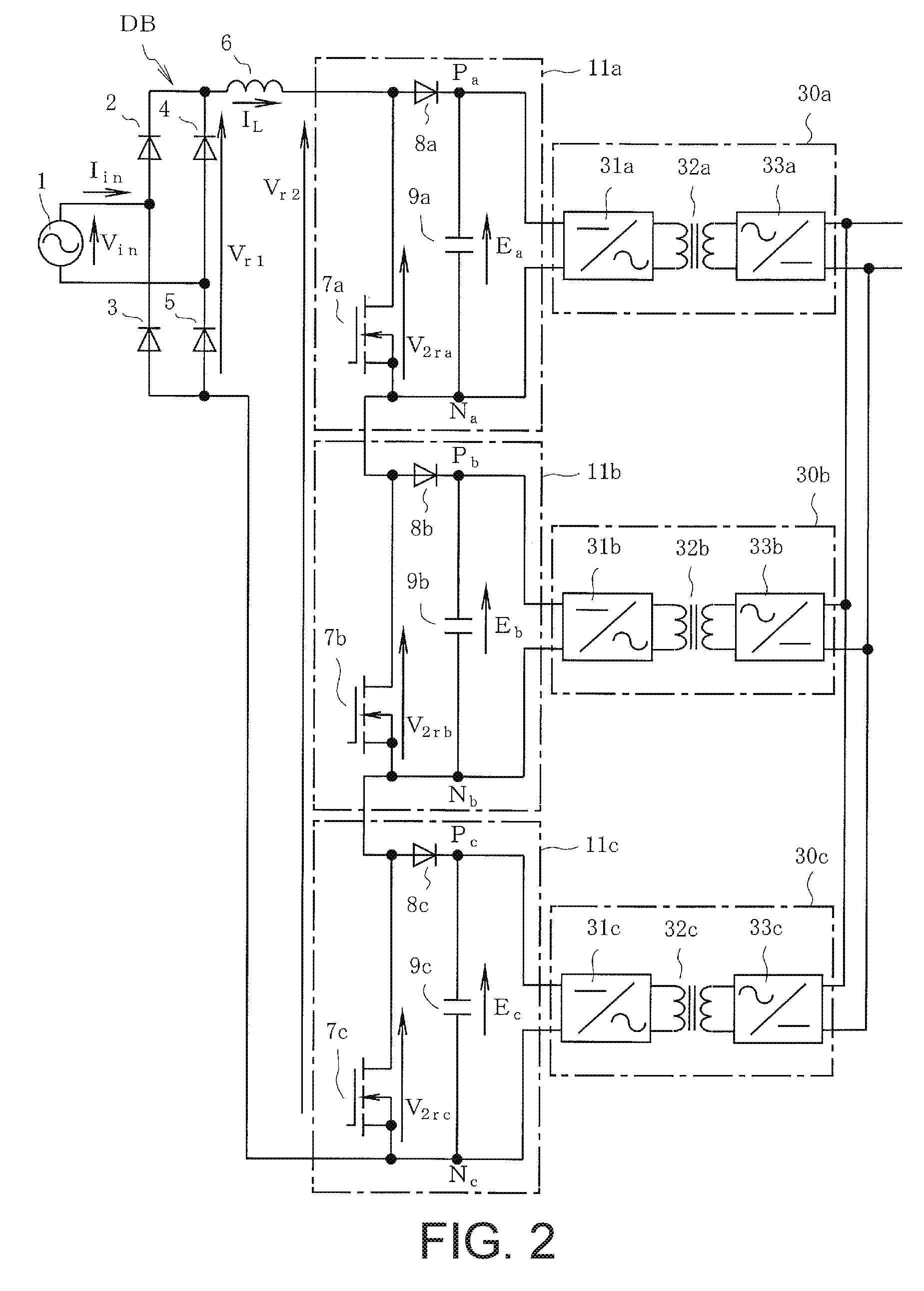
[0083]FIG. 2 shows Embodiment 2 of the present invention in which instead of the loads, DC-DC converter circuits are attached.

[0084]In FIGS. 2, 30a, 30b, and 30c are DC-DC converter circuits, and respectively replace the loads 10a, 10b, and 10c of FIG. 1. All other configurations are identical to those of FIG. 1.

[0085]In the DC-DC converter circuits 30a, 30b, and 30c: 31a, 31b, and 31c are DC-AC converting parts, 32a, 32b, and 32c are transformers, and 33a, 33b, and 33c are AC-DC converting parts (rectifiers). While not shown in the diagram, DC loads are respectively connected to the output sides of the AC-DC converting parts 33a, 33b, and 33c.

[0086]In general, the output frequencies of the DC-AC converting parts 31a, 31b, and 31c are set to a few kHz to a few dozen kHz or more in order to keep the transformers 32a, 32b, and 32c compact.

[0087]In Embodiment 2, the output sides of the AC-DC converting parts 33a, 33b, and 33c are connected together in parallel. On the other hand, the ...

embodiment 3

[0093]In addition, in Embodiment 3, while the frequencies of carriers a, b, and c generated by carrier generators 113a, 113b, and 113c are identical to one another, the phases of the carriers a, b, and c are different from one another as shown in FIG. 4. Here, since there are three groups of the switching units, 11a, 11b, and 11c, the phase difference among the carriers a, b, and c is 360° / 3=120° in electrical angle.

[0094]Note that in FIG. 4, an instantaneous value command of a Vr2 is illustrated for each of the carriers a, b, and c. However, this is only done to facilitate understanding; in reality, there is only a single instantaneous value command for the Vr2. In addition, V2ra, V2rb, and V2rc in FIG. 4 respectively represent input voltages of the switching units 11a, 11b, and 11c of FIGS. 1 and 2, and correspond to PWM pulses of the switching devices 7a, 7b, and 7c.

[0095]As described above, the phases of the carriers a, b, and c are different from one another. As a result, the ...


PUM


Abstract

An AC to DC converter includes a plurality of rectifier circuits connected in series to an AC voltage source at an input side to collectively receive an output voltage of the AC voltage source; and a plurality of switching units respectively connected to the plurality of rectifier circuits, each of the switching units having a semiconductor switching device, a diode, and a capacitor, and performing ON/OFF switching of the semiconductor switching device provided therein to step up a voltage received from the corresponding rectifier circuit, each of the switching units supplying the stepped-up voltage to said capacitor through said diode so that a resulting DC across said capacitor can be provided, as a DC output voltage of the switching unit, to a respective load to be connected to terminals of said capacitor.

Description

BACKGROUND OF THE INVENTION[0001]1. Technical Field[0002]The present invention relates to AC-DC converters.[0003]2. Background Art[0004]FIG. 10 is a circuit diagram of a conventional AC-DC converter, a circuit well known as a PFC (Power Factor Correction) circuit.[0005]In FIG. 10, 1 is an AC power source; 2 to 5 are diodes constituting a rectifier circuit (diode bridge) DB; 6 is an inductor; 7 is a semiconductor switching device; 8 is a diode; 9 is a capacitor; and 10 is a load. The portion constituted by the inductor 6, the switching device 7, the diode 8, and the capacitor 9 is also known as a so-called boost converter, which boosts a DC voltage to increase output. Other than the MOSFET (Metal Oxide Silicon Field Effect Transistor) shown here in the diagram, an IGBT (Isolated Gate Bipolar Transistor), a BJT (Bipolar Junction Transistor), or the like may also be used for the switching device 7.[0006]Note that in FIG. 10, Vin is an AC input voltage; Iin is an AC input current; IL is...

Claims


Application Information

Patent Timeline
IPC IPC(8): H02M3/156H02M7/06H02M3/04
CPCH02M3/156H02M3/04H02M2001/0074H02M2001/007H02M7/06H02M7/10H02M1/0043H02M1/007H02M1/0074
Inventor YAMADA, RYUJI
Owner FUJI ELECTRIC CO LTD
Why Eureka
Try Eureka