Dual-junction optical modulator and the method to make the same

a dual-junction, optical modulator technology, applied in non-linear optics, instruments, optics, etc., can solve the problems of lack of planar integration, lack of scalable manufacturing process, and high cost of devices made of these materials, so as to increase the overlap with the optical mode, increase the modulation efficiency, and reduce the effect of reducing the width of both junctions

Inactive Publication Date: 2016-10-27
LAXENSE
View PDF2 Cites 23 Cited by
  • Summary
  • Abstract
  • Description
  • Claims
  • Application Information

AI Technical Summary

Benefits of technology

[0012]The optical device further comprises a first heavily doped region below the first metal contact and a second heavily doped region below the second metal contact for better Ohmic contact.
[0013]In both embodiments, the two P-N junctions are connected in parallel with the same anode metal contact and cathode metal contact to form a dual-junction diode. The depletion widths of both junctions may be changed by varying an applied reverse voltage applied between the first and the second metal contacts. The two depletion regions, where the free carrier concentration changed with applied voltage, increase the overlap with the optical mode compared to the single P-N junction in a relatively larger waveguide therefore increase the modulation efficiency.

Problems solved by technology

However, devices made of these materials tend to be expensive and lack capability of planar integration and a scalable manufacturing process such as the ubiquitous silicon wafer fabrication process.

Method used


Image

  • Dual-junction optical modulator and the method to make the same
  • Dual-junction optical modulator and the method to make the same
  • Dual-junction optical modulator and the method to make the same

Examples


Embodiment Construction

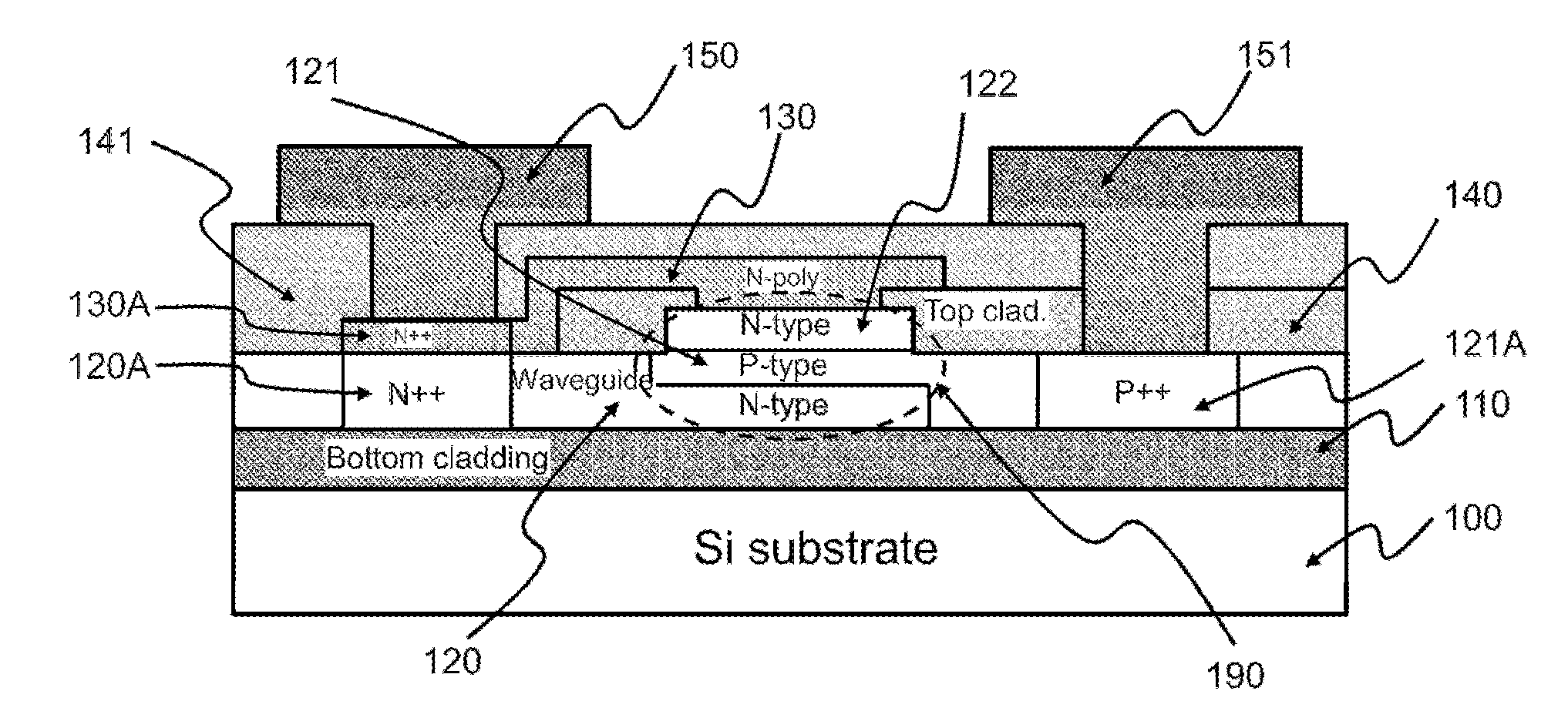
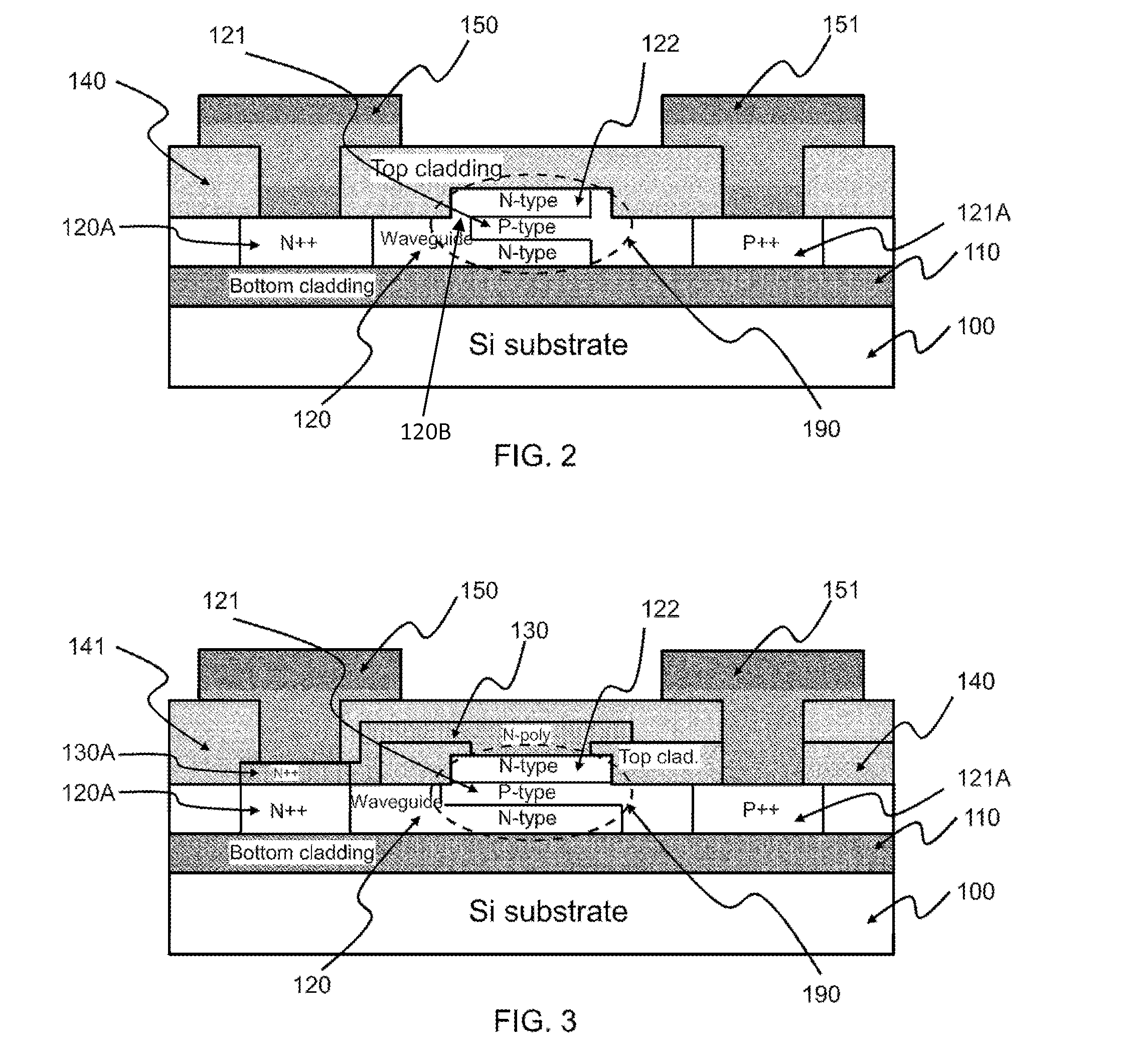
[0024]The invention relates to an optical device, in particular, a silicon or SiGe optical modulator using a rib waveguide structure fabricated on a substrate, and methods of making the same.

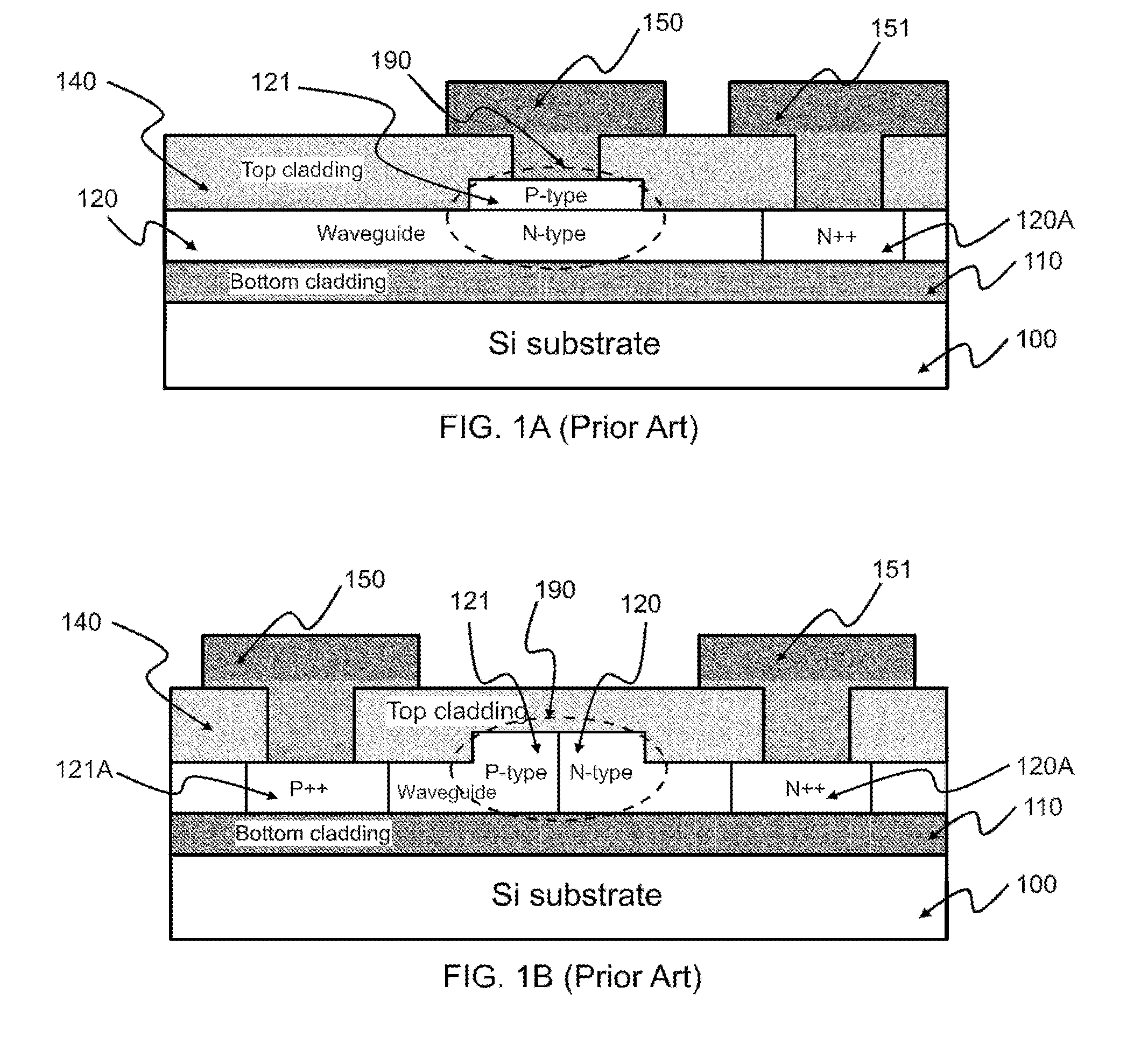
[0025]FIG. 1A and FIG. 1B schematically illustrates two prior arts rib waveguide silicon modulators using a vertical P-N diode and a horizontal P-N diode, respectively. It is known that the modulation efficiency of a carrier depletion modulator highly depends on the overlap of the carrier depletion region the PN junction and the optical mode 190. The P-N junction in both modulator designs in FIGS. 1A and 1B is located near the center of the optical mode. Nevertheless the depletion width is generally limited to less than 0.2 μm due to the choice of relatively high doping concentration in both P region 121 and N region 120 for better free carrier concentration changes by varying applied voltage between two metal contacts 150 and 151. When the optical mode is significantly larger than 0.2 μm due to...


PUM

PropertyMeasurementUnit
depletion widthaaaaaaaaaa
optical mode sizeaaaaaaaaaa
shift lengthaaaaaaaaaa

Abstract

An optical device includes a substrate and an optical rib waveguide structure formed of a slab and a rib. A vertically-oriented P-N-P or N-P-N dual-junction diode is formed inside the rib waveguide, including a first doped region, a second doped region and a third doped region electrically connected to the first doped region, where two P-N junctions are formed at the boundaries of the first and the second doped regions, and the second and the third doped regions, respectively. The depletion regions of the two junctions are substantially in the center of a guided optical mode propagating at the core region through the rib waveguide. The optical device further includes a first metal contact and a second metal contact in electrical contact with the first doped region and the second doped region, respectively.

Description

BACKGROUND OF THE INVENTION1. Field of the Invention[0001]The invention relates generally to optical devices. In particular, the invention relates to semiconductor based optical modulators.[0002]2. Description of the Related Art[0003]Optical modulators are key components in optical communication systems. Optical modulators are devices that convert electrical signals to optical signals. An optical modulator is traditionally made of bulk crystalline optical materials such as lithium niobate (LiNO3) that have strong electro-optic effects. However, devices made of these materials tend to be expensive and lack capability of planar integration and a scalable manufacturing process such as the ubiquitous silicon wafer fabrication process. The ever-increasing demands for communication bandwidth require low-cost highly-integrated optical devices. Silicon photonics is an emerging technology that can provide a solution. As a key component, optical modulators made of silicon are highly demanded....

Claims


Application Information

Patent Timeline
Patent Type & Authority Applications(United States)
IPC IPC(8): G02F1/025
CPCG02F2001/0151G02F1/025G02F1/0151G02F2201/063G02F2202/104G02F2203/50
Inventor SUN, XIAOCHENFENG, NINGNING
Owner LAXENSE
Why Eureka
Try Eureka