Radiation detector and method for reducing the amount of trapped charge carriers in a radiation detector

a radiation detector and charge carrier technology, applied in radiation intensity measurement, radiation measurement, instruments, etc., can solve the problems of reducing the sensitivity of the detector, restricting the range of external optical energy sources usable, and reducing the residual net free carrier concentration, so as to reduce the amount of charge carriers and improve the signal-to-noise ratio , the effect of efficient recombination

Active Publication Date: 2017-01-05
XCOUNTER
View PDF0 Cites 0 Cited by
  • Summary
  • Abstract
  • Description
  • Claims
  • Application Information

AI Technical Summary

Benefits of technology

[0025]This means that the repetition rate of the detector can be kept high; the exposing of the substrate of semiconductor material for light does not affect the repetition rate et all since it is performed during already existing readout periods. Such solution can not be performed with the detector disclosed in EP 1018655 B1 since it is accumulating charges and such detector would be affected by the freed charges, which would cause the readout to be deteriorated or even useless. In the aspect above, a photon counting detector is used, and in this detector the pixels are “locked” during readout and consequently the freed charges from the light exposure would not affect the readout.
[0029]A cyclic detector bias voltage, which is only applied over the substrate during the periods of time, during which the radiation detector is used for detecting radiation, i.e. i.e. the above data acquisition period, will further reduce amount of charge carriers that get trapped at deep-level defects in the substrate of the detector.
[0030]Also, the absence of the detector bias voltage during the exposure of the substrate for the light enable efficient recombination of released negative and positive charge carriers.
[0031]An advantage of this aspect is that no measurement frames are “lost”, and the total measurement time will not increase. On the other hand, it puts higher requirements on the switching speed of the light and the detector bias voltage. In some applications wherein the repetition rate may be 1 kHz or higher, hardware limitations may restrict the use of this aspect.

Problems solved by technology

A problem with the semiconductors is the occurrence of deep-level defects within the doped semiconductors, which may capture charge carriers and reduce the residual net free carrier concentration.
These trapped negative and positive charge carriers cause a space-charge formation and affect the overall electric field in the semiconductor and may cause noise.
However, a drawback with the approach of US 2010 / 0078559 A1 is that it requires that the crystals of the detector are transparent to the light of the external optical energy source allowing no additional absorption.
This may restrict the range of external optical energy sources usable.
A further drawback is that the sensitivity of the detector may be reduced since the released charge carriers will be mixed with the charge carriers created via interaction between the radiation to be detected and the crystals of the detector and interfere with the detection.
This may not normally be a problem, but at low radiation flux, the released charge carriers may cause non-acceptable deterioration of the detection sensitivity.
A yet further drawback is that released negative and positive charge carriers do not recombine efficiently, which will further reduce the detector sensitivity.
A still further drawback is that the exposure of the crystals for the infrared light radiation increases the dark current of the detector.
However, such procedure is not applicable to imaging at very high repetition rates since each frame contains a further time period t6-t5 with the only purpose of illuminating the panel with radiation, such as visible radiation, preferably from both sides.
Such solution can not be performed with the detector disclosed in EP 1018655 B1 since it is accumulating charges and such detector would be affected by the freed charges, which would cause the readout to be deteriorated or even useless.
In some applications wherein the repetition rate may be 1 kHz or higher, hardware limitations may restrict the use of this aspect.

Method used


Image

  • Radiation detector and method for reducing the amount of trapped charge carriers in a radiation detector
  • Radiation detector and method for reducing the amount of trapped charge carriers in a radiation detector
  • Radiation detector and method for reducing the amount of trapped charge carriers in a radiation detector

Examples


Embodiment Construction

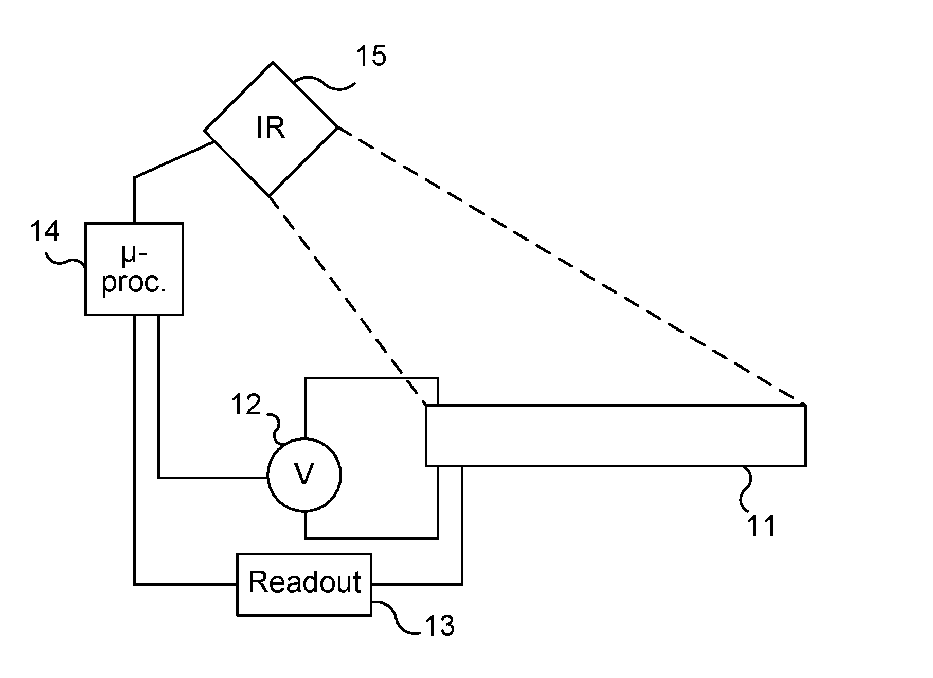
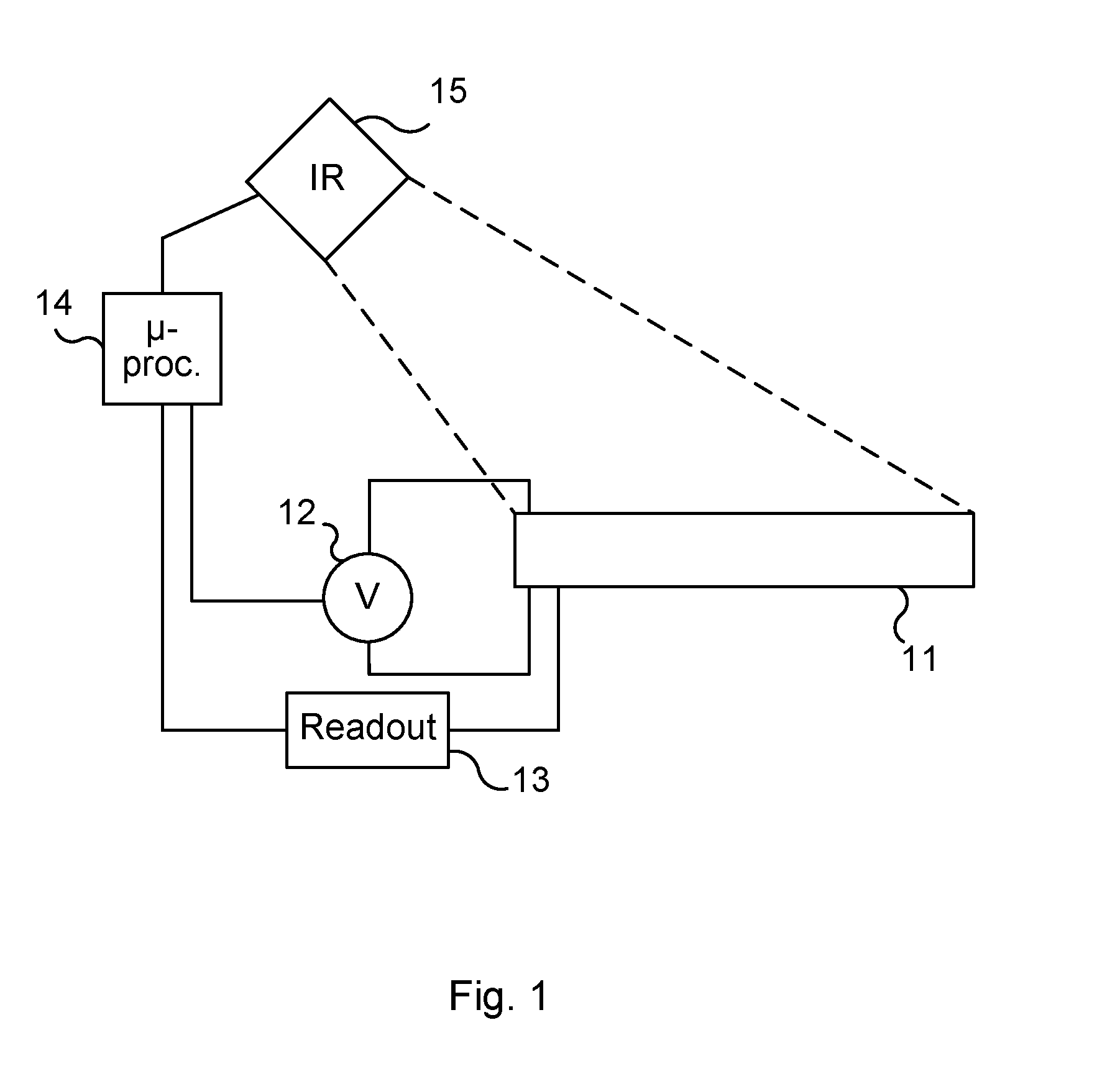
[0050]FIG. 1 illustrates, schematically, a semiconductor based X ray or gamma ray radiation detector according to one embodiment. The radiation detector comprises a substrate 11 of semiconductor material, a detector bias voltage supply 12 for applying a detector bias voltage over the substrate, a readout arrangement 13 for reading out data indicative of charges freed in, and transported through, the substrate 11, and a control device 14 operatively connected to the detector bias voltage supply 12 and the readout arrangement 13 for controlling the same. The radiation detector may be a Cd—Te or Cd—Zn—Te based radiation detector.

[0051]Examples of detector layouts and substrate materials are further disclosed in U.S. Pat. No. 5,379,336; U.S. Pat. No. 6,933,505; U.S. Pat. No. 7,170,062; U.S. Pat. No. 7,189,971; U.S. Pat. No. 7,361,881; US 2006 / 011853; US2006 / 071174; and US2008 / 019477, the contents of which being hereby incorporated by reference.

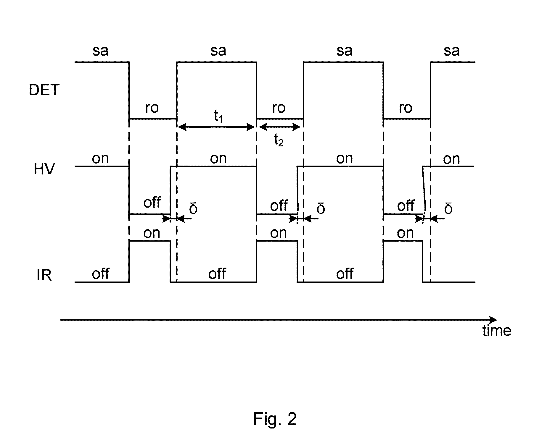
[0052]The radiation detector further compri...


PUM


Abstract

A semiconductor based photon counting detector comprising a substrate (11) of semiconductor material; a detector bias voltage supply (12) for applying a detector bias voltage over the substrate, each time during a data acquisition period (t1); a readout arrangement (13) for repetitively reading out data indicative of charges freed in, and transported through, the substrate (11) in response to photons being absorbed, each time during a readout period (t2) following a data acquisition period, wherein the data contain number of charge pulses of photons being absorbed; an external light source (15) for exposing the substrate for light to enable trapped charge carriers to escape from defect levels in the substrate; and a control device (14) operatively connected to the detector bias voltage supply, the readout arrangement, and the external light source. The control device (14) is configured to control the detector bias voltage supply to switch off the detector bias voltage over the substrate and the external light source (15) to switch on the light, thus exposing the substrate (11) for light to enable trapped charge carriers to escape from defect levels in the substrate, concurrently during at least some of said readout periods.

Description

TECHNICAL FIELD[0001]The technical field relates to semiconductor based X ray or gamma ray radiation detectors.DESCRIPTION OF RELATED ART[0002]In semiconductor detectors, the detector consists of a slab of semiconductor material with electrodes on the opposite faces of the semiconductor. The detector material is depleted in free carriers and a high voltage electric field is applied between the electrodes using an outside bias. High-energy photons from an outside radioactive source or x-ray tube induce electron-hole pairs in the semiconductor volume through photoelectric or Compton interactions. The interaction is a two-step process where the high-energy electrons created in the photoelectric or Compton event lose their energy through repeated electron-hole ionization. Due to the high cross section of this process, the electron-hole pairs form a highly localized charge cloud only few micro-meters in diameter.[0003]One important aspect of the photon interaction for imaging is that the...

Claims


Application Information

Patent Timeline
Patent Type & Authority Applications(United States)
IPC IPC(8): G01T1/24G01T1/18
CPCG01T1/24G01T7/005G01T1/18
Inventor ULLBERG, CHRISTERURECH, MATTIASWEBER, NICLAS
Owner XCOUNTER
Why Eureka
Try Eureka