Atomic layer deposition apparatus and atomic layer deposition system

Inactive Publication Date: 2017-01-12
APPLIED MATERIALS INC
View PDF4 Cites 5 Cited by
  • Summary
  • Abstract
  • Description
  • Claims
  • Application Information

AI Technical Summary

Benefits of technology

[0020]According to the present invention, the atomic layer deposition apparatus and the atomic layer deposition system may reduce the installation space for the apparatus and significantly improve the production speed by forming the thin film on the surface of the substrate by the relative rotation with respect to the gas injection unit in the state in which the plurality of substrates are supported by one substrate support unit in one vacuum chamber.
[0021]Especially, the conventional atomic layer deposition apparatus, which deposits the thin film by using the linear movement of the substrate when the atomic layer deposition process is performed, performs the substrate processing for one substrate at a time and secure the space for linear movement of the substrate. However, the atomic layer deposition apparatus and the atomic layer deposition system according to the present invention may process two or more substrates in one vacuum chamber to maximize the space efficiency of the apparatus.
[0022]Also, the conventional atomic layer deposition apparatus, which deposits the thin film by using the linear movement of the substrate when the atomic layer deposition process is performed, has a limitation in reducing the distance between the source gas injection unit and the reaction gas injection unit due to particle generated by reaction between the source gas and the reaction gas. However, the atomic layer deposition apparatus and the atomic layer depositio

Problems solved by technology

However, a light emitting layer of an organic electroluminescent device can be damaged when exposed to moisture and oxygen.
However, as the conventional atomic layer deposition apparatus, which forms the thin film on a surface of the substrate by spraying the source gas and the reaction gas w

Method used


Image

  • Atomic layer deposition apparatus and atomic layer deposition system
  • Atomic layer deposition apparatus and atomic layer deposition system
  • Atomic layer deposition apparatus and atomic layer deposition system

Examples


Example

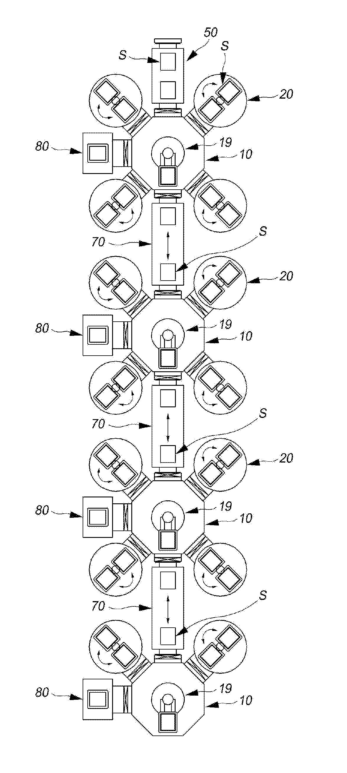
[0048]As shown in FIG. 1, an atomic layer deposition system according to a first embodiment of the present invention may include at least one transfer apparatus 10 in which a transfer robot 19 is installed and a plurality of atomic layer deposition apparatuses each of which is coupled to the transfer apparatus 10 to receive a substrate S by the transfer robot 19.

[0049]The transfer apparatus 10 transfers the substrate S to each of the atomic layer deposition apparatuses 20. The transfer apparatus 10 may be variously provided.

[0050]The transfer apparatus 10 according to an embodiment may include a transfer chamber to which the atomic layer deposition apparatuses 20 are coupled and the transfer robot 19 installed in the transfer chamber to transfer the substrate S.

[0051]The transfer chamber provides a space for installing the transfer robot 19 and a sealed space capable of maintaining a vacuum pressure that is almost the same as that of the atomic layer deposition apparatus 20. The tra...

Example

[0056]As shown in FIG. 10, an atomic layer deposition system according to a second embodiment of the present invention may include a plurality of transfer apparatuses 10 in which the transfer robots 19 are respectively installed and which are arranged in a line and a plurality of atomic layer deposition apparatuses 20 respectively arranged between the plurality of transfer apparatuses 10 to receive the substrate S by the transfer robot 19.

[0057]The atomic layer deposition system according to the second embodiment of the present invention is the same as or similar to the first embodiment except that the transfer apparatus 10 and the atomic layer deposition apparatus 20 are sequentially, i.e., inline, installed. Detailed description for this will be omitted.

[0058]In the atomic layer deposition system according to the second embodiment, the atomic layer deposition apparatus 20 may perform two or more thin film deposition processes at a time to have a small installation space and quickl...

Example

[0061]An atomic layer deposition system according to a third embodiment of the present invention is an example in which the atomic layer deposition apparatus 20 according to the present invention, which will be described later, and a linear movement atomic layer deposition apparatus 40 performing a substrate processing while linearly moving the substrate S are combined.

[0062]In detail, as shown in FIG. 11, in the atomic layer deposition system according to the third embodiment of the present invention, the linear movement atomic layer deposition apparatus 40 for linearly moving the substrate S and performing the substrate processing may be additionally coupled to the transfer apparatus 10 of the atomic layer deposition system according to the first embodiment, or the transfer chamber 30 to which only at least one linear movement atomic layer deposition apparatus 40 for linearly moving the substrate S and performing the substrate processing is coupled may be further provided.

[0063]As...


PUM


Abstract

An atomic layer deposition apparatus and an atomic layer deposition system, capable of reducing space for installing the apparatus and significantly improving production speed by forming a thin film on a surface of each of a plurality of rectangular substrates by rotating the substrates with respect to a gas spray portion, with the substrates being supported by one substrate support portion. The atomic layer deposition apparatus includes: a vacuum chamber; a gas supply portion, which is provided above or below the vacuum chamber, and which supplies gas so that a thin film is deposited on a surface of each of substrates; and a substrate support portion, which is provided in the vacuum chamber so as to horizontally rotate about the gas supply portion, and which supports the two or more rectangular substrates arranged in the circumferential direction with respect to the center of rotation of the substrate support portion.

Description

CROSS-REFERENCE TO RELATED APPLICATIONS[0001]This U.S. non-provisional patent application claims priority under 35 U.S.C. §119 of Korean Patent Application Nos. 10-2014-0023002, filed on Feb. 27, 2014, 10-2014-0136990, filed on Oct. 10, 2014, and 10-2014-0141252, filed on Oct. 18, 2014, the entire contents of which are hereby incorporated by reference.TECHNICAL FIELD[0002]The present invention disclosed herein relates to an atomic layer deposition apparatus and an atomic layer deposition system.BACKGROUND ART[0003]An organic electroluminescent display device is a self-light emitting type display electrically exciting a fluorescent organic compound to emit light. The organic electroluminescent display device is being spotlighted as a next generation display because it can be driven at a low voltage and easily manufacture in slim, and have a wide viewing angle and a quick response speed.[0004]However, a light emitting layer of an organic electroluminescent device can be damaged when e...

Claims


Application Information

Patent Timeline
IPC IPC(8): C23C16/455C23C16/04C23C16/44C23C16/458H01L51/56H01L51/52
CPCC23C16/45544H01L51/56C23C16/042C23C16/4412C23C16/458H01L51/5253C23C16/403C23C16/45551C23C16/4584H10K50/844H10K71/00H01L21/682H10K71/166C23C14/042
Inventor CHO, SAENG HYUN
Owner APPLIED MATERIALS INC
Why Eureka
Try Eureka