Manufacturing method of TFT substrate structure

a manufacturing method and substrate technology, applied in the field of display technology, can solve problems such as negative influence on the quality of tft substrates, and achieve the effects of reducing production costs, preventing the reduction of aperture ratio, and improving production efficiency

Active Publication Date: 2017-01-19
SHENZHEN CHINA STAR OPTOELECTRONICS TECH CO LTD
View PDF0 Cites 5 Cited by
  • Summary
  • Abstract
  • Description
  • Claims
  • Application Information

AI Technical Summary

Benefits of technology

[0053]The efficacy of the present invention is that the present invention provides a manufacturing method of a TFT substrate structure, which comprises sequentially forming a first passivation layer, a planarization layer, and a first transparent conductive film and then first subjecting the first transparent conductive film to patterning to form a first pixel electrode and thereafter, a photolithographic process is applied to the planarization layer for exposure and thus forming a first via located above and corresponding to a drain terminal,...

Problems solved by technology

wherein since the portion of the first transparent conductive film located in the first and second vias 810, 910 may be covered by residues of the photoresist, it may not be completely removed in the etching proc...

Method used


Image

  • Manufacturing method of TFT substrate structure
  • Manufacturing method of TFT substrate structure
  • Manufacturing method of TFT substrate structure

Examples


Embodiment Construction

[0074]To further expound the technical solution adopted in the present invention and the advantages thereof, a detailed description is given to a preferred embodiment of the present invention and the attached drawings.

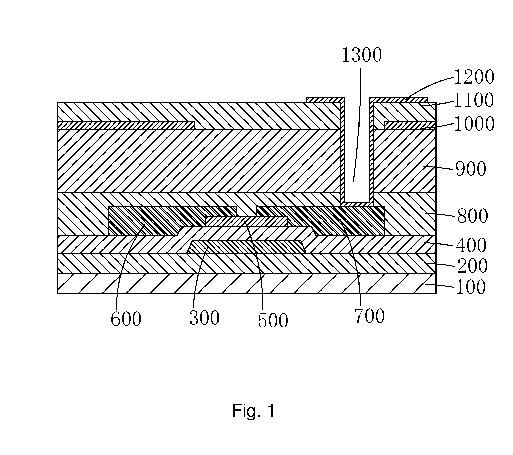
[0075]Referring to FIG. 10, the present invention provides a manufacturing method of a thin-film transistor (TFT) substrate structure, which comprises the following steps:

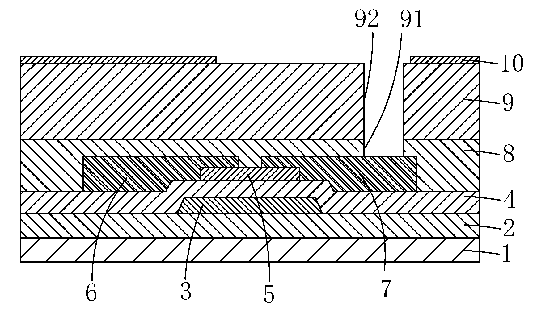
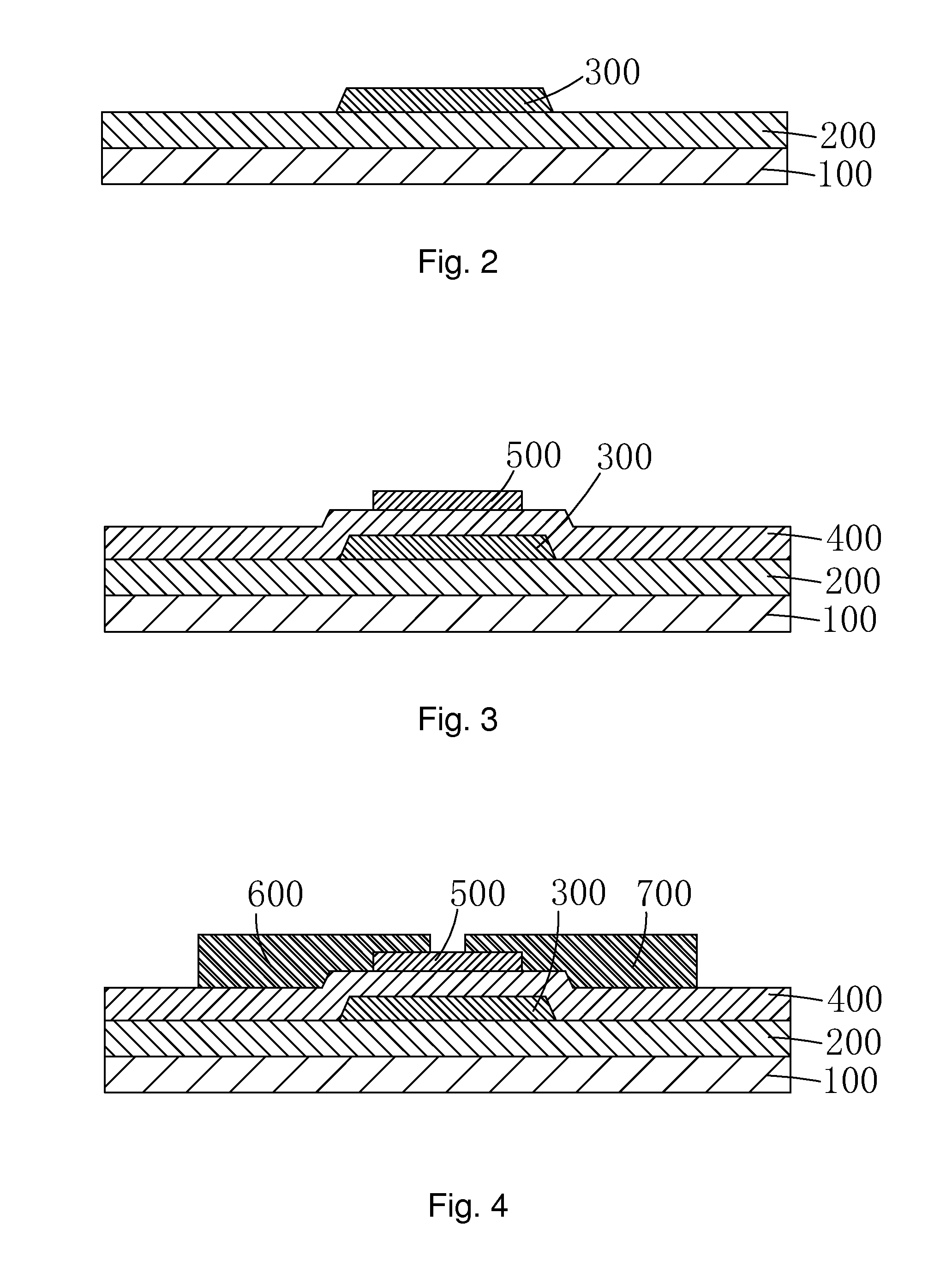
[0076]Step 1: as shown in FIG. 11, providing a base plate 1 and depositing a buffer layer 2 on the base plate 1 and depositing a first metal layer on the buffer layer 2 and subjecting the first metal layer to patterning to form a gate terminal 3.

[0077]Preferably, the gate terminal 3 comprises a material of one of molybdenum, titanium, aluminum, and copper or a stacked combination of multiple ones thereof.

[0078]Step 2: as shown in FIG. 12, depositing a gate insulation layer 4 on the buffer layer 2 and the gate terminal 3 and depositing an oxide semiconductor on the gate insulation layer 4 and subjectin...


PUM


Abstract

The present invention provides a manufacturing method of a TFT substrate structure, which includes sequentially forming a first passivation layer, a planarization layer, and a first transparent conductive film and then first subjecting the first transparent conductive film to patterning to form a first pixel electrode and thereafter, a photolithographic process is applied to the planarization layer for exposure and thus forming a first via located above and corresponding to a drain terminal, followed by using the planarization layer as a self-aligning mask to apply dry etching to the first passivation layer for etching to form a second via that corresponds to the first via, whereby residues of the first transparent conductive film in the first and second vias can be effectively prevented and product yield is enhanced. Further, on mask can be saved to prevent reduction of aperture ratio caused by misalignment thereby improving the production efficiency, reducing production cost, and increasing cost-related competition power of products.

Description

BACKGROUND OF THE INVENTION[0001]1. Field of the Invention[0002]The present invention relates to the field of display technology, and in particular to a manufacturing method of a thin-film-transistor (TFT) substrate structure.[0003]2. The Related Arts[0004]A liquid crystal display (LCD) comprises an enclosure, a liquid crystal panel arranged in the enclosure, and a backlight module mounted in the enclosure. The liquid crystal panel is generally composed of a color filter (CF) substrate, a thin-film transistor (TFT) array substrate, and a liquid crystal layer filled between the two substrates. The CF substrate and the TFT substrate have inner surfaces facing each other and provided with transparent electrodes. The liquid crystal display is operated by providing an electric field to control the direction of liquid crystal molecules in order to change the state of polarization, and polarizers are involved to selectively to allow an optic path to pass or be blocked to thereby achieve th...

Claims


Application Information

Patent Timeline
IPC IPC(8): H01L27/12H01L29/66
CPCH01L27/1262H01L27/1225H01L29/66969H01L21/768H01L21/77H01L29/78636H01L29/7869H01L27/1248
Inventor LV, XIAOWEN
Owner SHENZHEN CHINA STAR OPTOELECTRONICS TECH CO LTD
Why Eureka
Try Eureka