

Thin-film transistor and manufacturing method thereof
a technology of thin film transistor and manufacturing method, which is applied in the direction of transistors, semiconductor devices, electrical devices, etc., can solve the problems of limiting the application of thin film in pixel switches, adverse effects on component properties, and conventional active layer materials that cannot meet the requirements of such high-resolution displays, and achieves low uniformity problems, high carrier mobility, and high current on/off ratio
- Summary
- Abstract
- Description
- Claims
- Application Information
AI Technical Summary
Benefits of technology
Problems solved by technology
Method used
Image

Examples
Embodiment Construction
[0026]The present invention provides a thin-film transistor and a manufacturing method thereof which incorporate the foregoing technical features and whose major effects are detailed below.
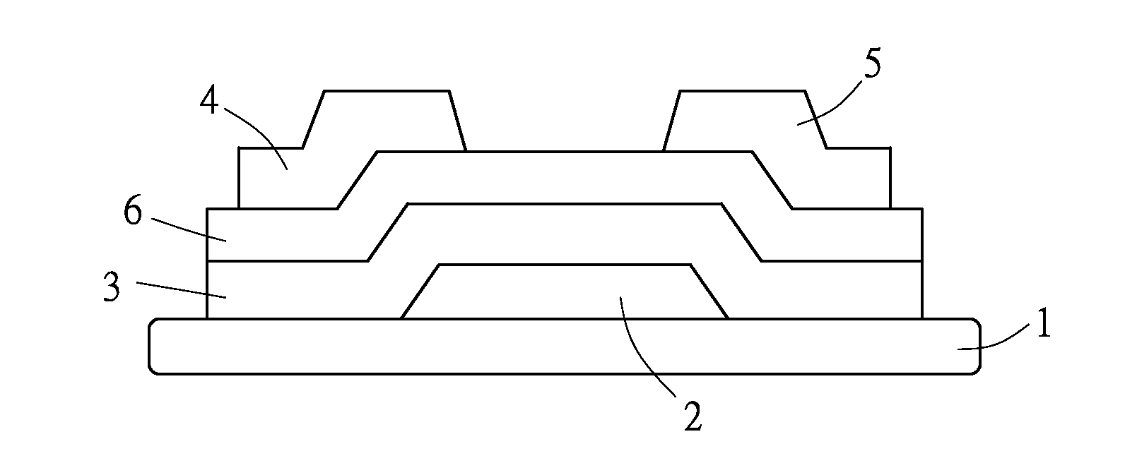
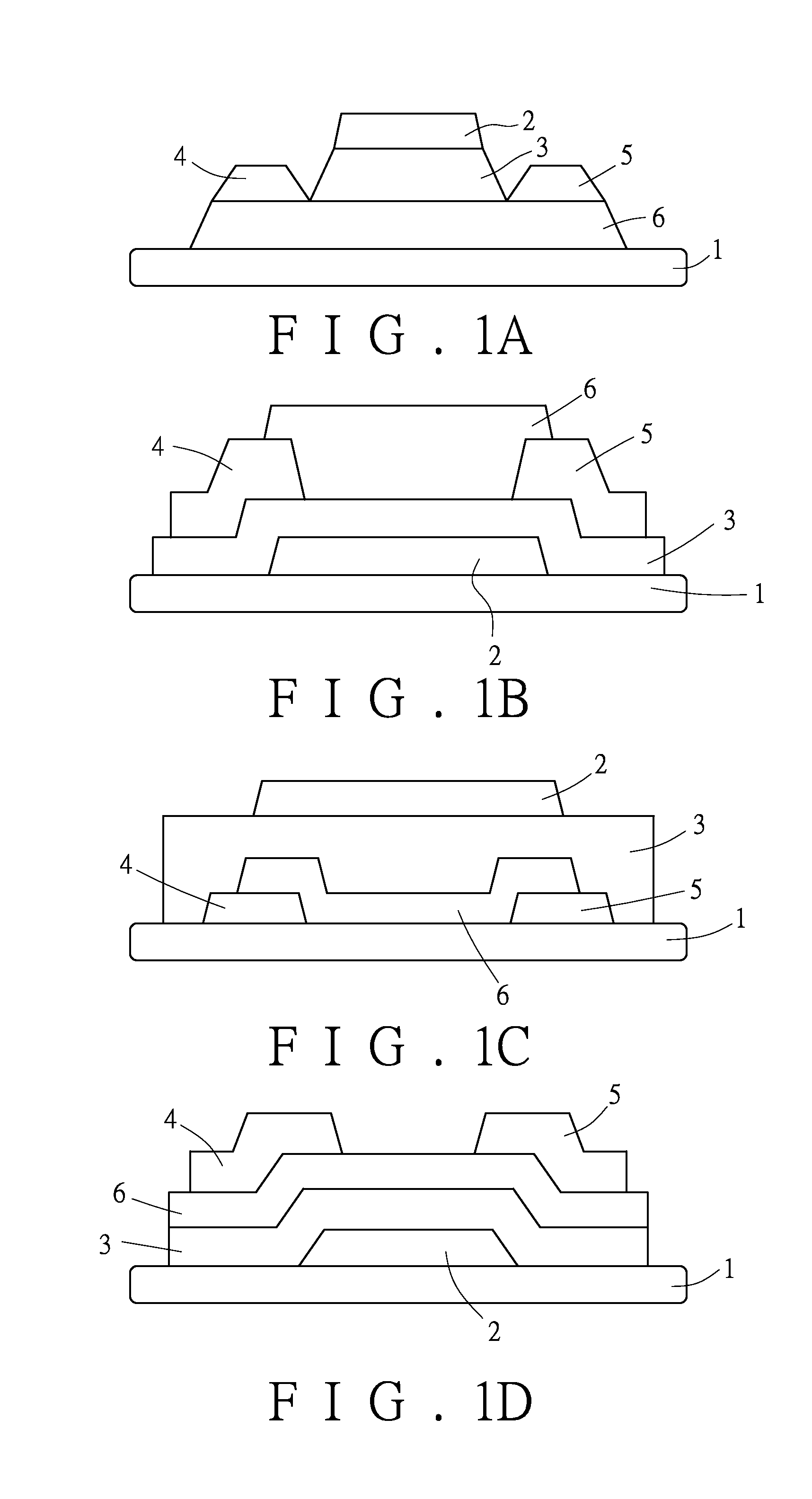
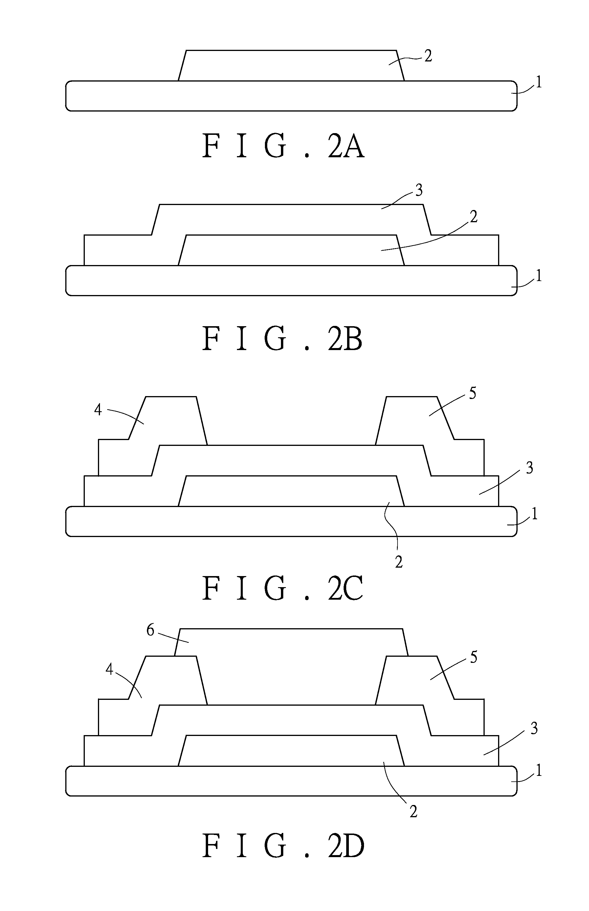
[0027]FIG. 1A to FIG. 1D show the thin-film transistors in four different embodiments of the present invention, wherein the thin-film transistors have a coplanar structure, an inverted coplanar structure, a staggered structure, and an inverted staggered structure respectively. All the four structures are well known in the art. Each of these thin-film transistors includes a substrate 1, a gate electrode 2, a gate electrode insulating layer 3, a source electrode 4, a drain electrode 5, and an active layer 6 stacked together, wherein the active layer is a group IV-VI compound semiconductor film. The group IV-VI compound can be any one of the following five compounds and their ternary, quaternary, or quinary compounds: GeS, GeSe, GeTe, SnSe, and SnTe. Each of the gate electrode 2, the source electrode...
PUM
 Abstract
Description
Claims
Application Information