Face-to-face semiconductor assembly having semiconductor device in dielectric recess

a semiconductor and dielectric recess technology, applied in semiconductor devices, semiconductor/solid-state device details, electrical apparatus, etc., can solve the problems of complex manufacturing process, inability to use in practical applications, and inability to reliably assemble, so as to reduce the interconnection distance

Inactive Publication Date: 2017-02-02
BRIDGE SEMICON
View PDF6 Cites 9 Cited by
  • Summary
  • Abstract
  • Description
  • Claims
  • Application Information

AI Technical Summary

Benefits of technology

[0005]A primary objective of the present invention is to provide a face-to-face semiconductor assembly having a bottom device positioned in a recess of a core base so that the displacement of the embedded bottom device can be controlled.
[0006]Another objective of the present invention is to provide a face-to-face semiconductor assembly having an array of metal posts formed in the core base for vertical interconnection. As both the recess and the metal posts originate from a same metal carrier, the pre-determined relative location between the metal posts and the embedded bottom device can be guaranteed.
[0007]Yet another objective of the present invention is to provide a face-to-face semiconductor assembly having both the recess and the metal posts enclosed in the core base. As the minimal height of the metal posts needed for the vertical connection between opposite sides of the core base can be compensated for by the amount equal to the depth of the recess, the manufacturing yield and cost can be greatly improved.
[0010]The face-to-face semiconductor assemblies according to the present invention have numerous advantages. For instance, face-to-face electrically coupling the first and second semiconductor devices to both opposite sides of the top buildup circuitry can minimize the interconnection distance between the first and second semiconductor devices. Inserting the first semiconductor device into the recess of the dielectric layer can reduce the minimal required height of the metal posts by the amount equal to the depth of the recess of the dielectric layer and offer a flat platform to proceed with face-to-face interconnection procedure for electrically coupling second semiconductor device to the top buildup circuitry.

Problems solved by technology

Since the bottom chip is not protected and has to be thinner than the solder ball(s) for external connection, the assembly is not reliable and cannot be used in practical applications.
Although there is no TSV in the stacked chips, the TSV in the interposer that serves for circuitry routing between chips induces complicated manufacturing processes, high yield loss and excessive cost.

Method used


Image

  • Face-to-face semiconductor assembly having semiconductor device in dielectric recess
  • Face-to-face semiconductor assembly having semiconductor device in dielectric recess
  • Face-to-face semiconductor assembly having semiconductor device in dielectric recess

Examples


embodiment 1

[0050]FIGS. 1-28 are schematic views showing a method of making a face-to-face semiconductor assembly that includes a first semiconductor device, a core base, a top buildup circuitry, a bottom buildup circuitry and a second semiconductor device in accordance with the first embodiment of the present invention.

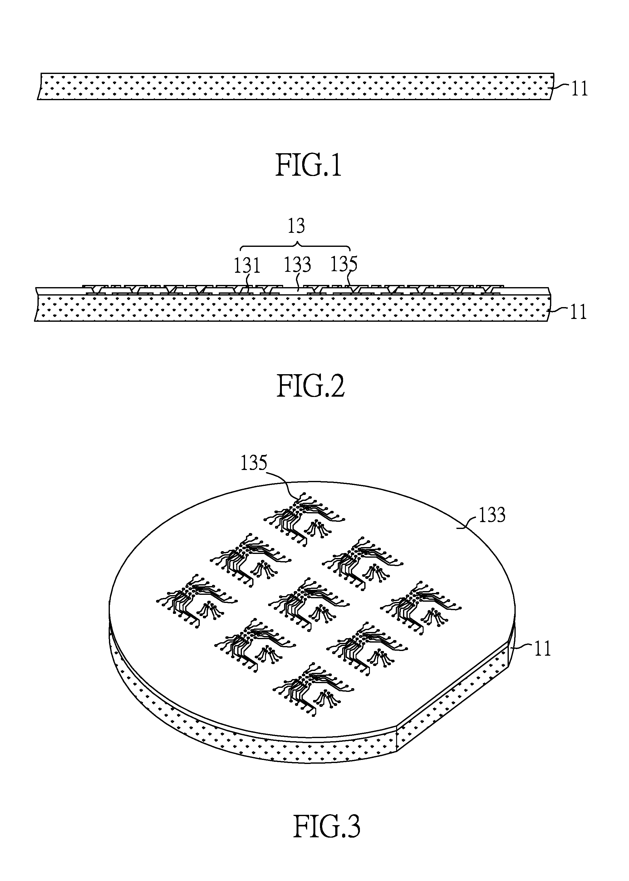
[0051]FIG. 1 is a cross-sectional view of a sacrificial carrier 11. The sacrificial carrier 11 can be made of any peelable or removable material, such as silicon, copper, aluminum, iron, nickel, tin or alloys thereof.

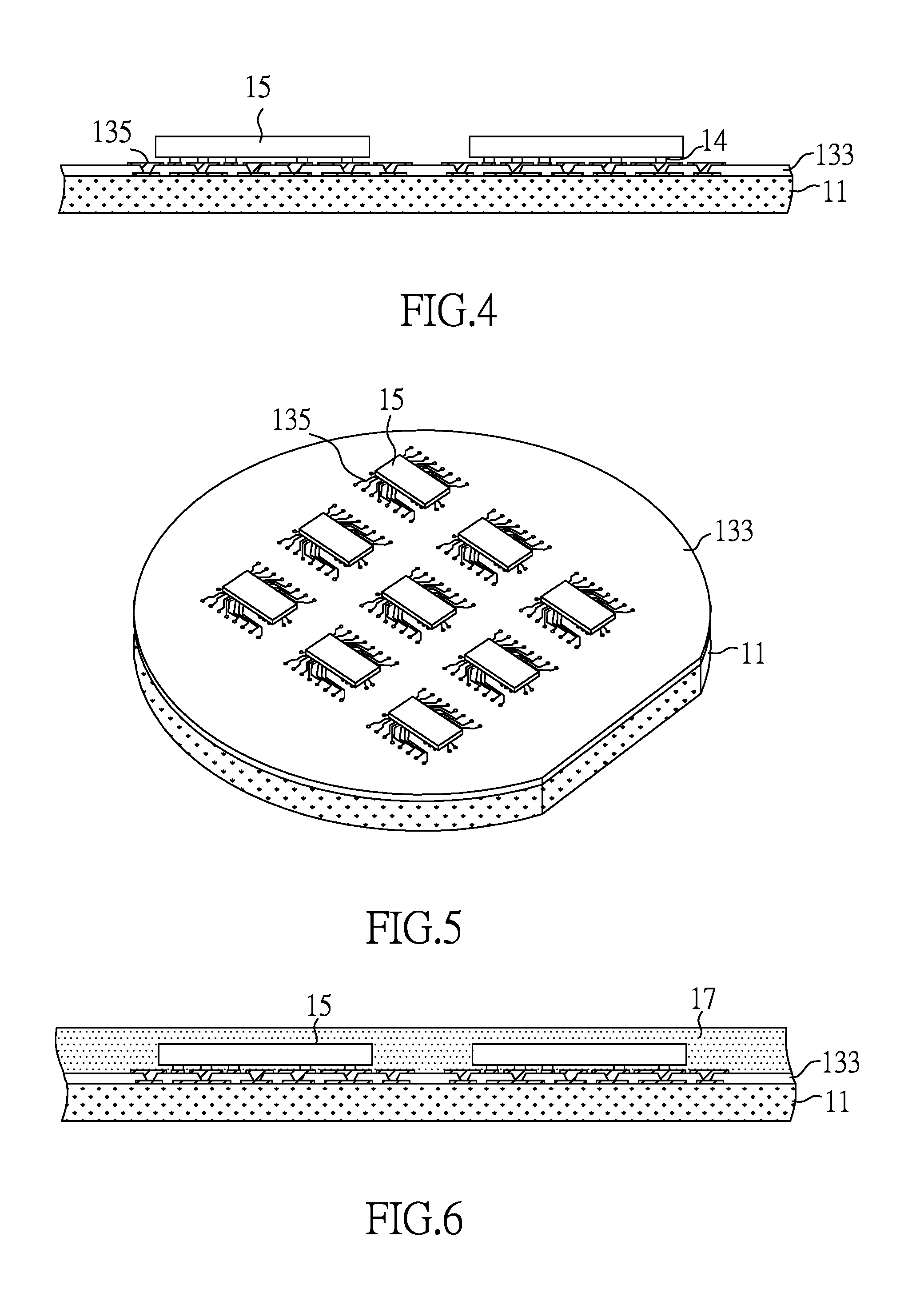
[0052]FIGS. 2 and 3 are cross-sectional and top perspective views, respectively, of the structure with a re-distribution layer 13 formed on the sacrificial carrier 11. In this illustration, the re-distribution layer 13 includes first routing traces 131, an insulating layer 133 and second routing traces 135. The first routing traces 131 extend laterally on the sacrificial carrier 11. The insulating layer 133 contacts and covers and extends laterally on the sacrificia...

embodiment 2

[0074]FIGS. 29-41 are schematic views showing a method of making a thermally enhanced face-to-face semiconductor assembly with a metal paddle deposited in the recess and auxiliary metal pads underneath the metal posts in accordance with the second embodiment of the present invention.

[0075]For purposes of brevity, any description in Embodiment 1 above is incorporated herein insofar as the same is applicable, and the same description need not be repeated.

[0076]FIG. 29 is a cross-sectional view of the structure with a protruded metal platform 221 and an array of auxiliary metal pads 223 formed on a metal carrier 21. The protruded metal platform 221 and the auxiliary metal pads 223 extend from the bottom surface of the metal carrier 21 in the downward direction. In this illustration, the auxiliary metal pads 223 are substantially coplanar with the protruded metal platform 221 at their top and bottom surfaces. The auxiliary metal pads 223 can be made of the same material as the protruded...

embodiment 3

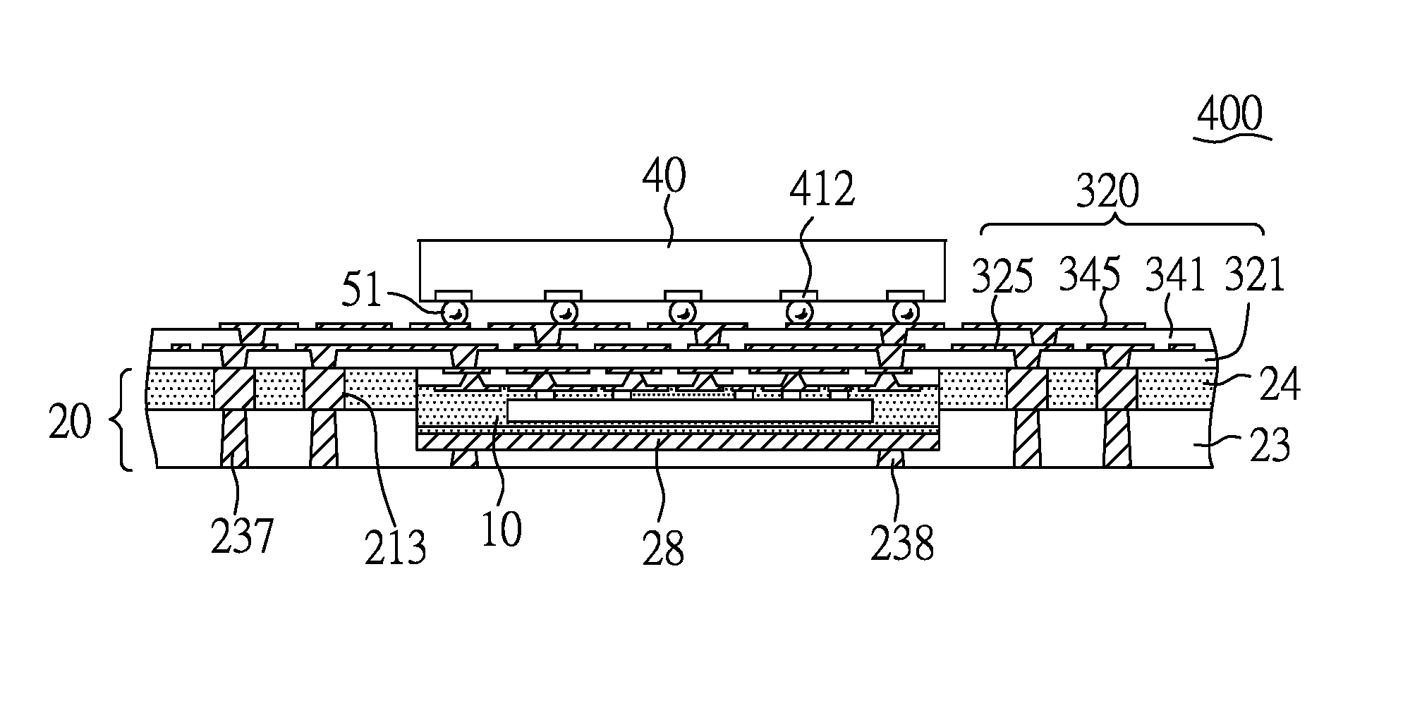
[0091]FIG. 42 is a cross-sectional view of another face-to-face semiconductor assembly 300 without bottom buildup circuitry in accordance with the third embodiment of the present invention.

[0092]In this embodiment, the face-to-face semiconductor assembly 300 is similar to that illustrated in Embodiment 1, except that no bottom buildup circuitry is formed on the bottom surface of the core base 20 and the core base 20 further includes an array of auxiliary metal pads 223 laterally covered by the first dielectric layer 23 and electrically coupled to and disposed between the metal posts 213 and the first metallized vias 237.


PUM


Abstract

A face-to-face semiconductor assembly is characterized by a semiconductor device positioned in a dielectric recess of a core base and surrounded by an array of metal posts. The recess in the core provides lateral displacement control between the device and the metal posts, and the minimal height of the metal posts needed for the vertical connection between both opposite sides of the core base can be reduced by the amount equal to the depth of the recess. Further, the semiconductor device is face-to-face electrically coupled to another semiconductor device through a buildup circuitry therebetween.

Description

CROSS REFERENCE TO RELATED APPLICATIONS[0001]This application is a continuation-in-part of U.S. application Ser. No. 14 / 957,954 filed Dec. 3, 2015. This application also claims the benefit of filing date of U.S. Provisional Application Ser. No. 62 / 198,058 filed Jul. 28, 2015. The entirety of each of said applications is incorporated herein by reference.FIELD OF THE INVENTION[0002]The present invention relates to a face-to-face semiconductor assembly, more particularly, to a face-to-face semiconductor assembly having a semiconductor device confined in a recess of a core base that includes an array of metal posts around the recess.DESCRIPTION OF RELATED ART[0003]Market trends of multimedia devices demand for faster and slimmer designs. One of assembly approaches is to interconnect two chips with “face-to-face” configuration so that the routing distance between the two chips can be the shortest possible. As the stacked chips can talk directly to each other with reduced latency, the ass...

Claims


Application Information

Patent Timeline
Patent Type & Authority Applications(United States)
IPC IPC(8): H01L25/065H01L23/498H01L23/31
CPCH01L25/0657H01L23/3107H01L23/49838H01L23/49894H01L2225/06589H01L23/49827H01L2225/06548H01L2225/06572H01L23/49822H01L23/52H01L21/561H01L21/568H01L2224/16227H01L2224/81005H01L2224/97H01L2924/15313H01L2225/06517H01L2224/81
Inventor LIN, CHARLES W.C.WANG, CHIA-CHUNG
Owner BRIDGE SEMICON
Why Eureka
Try Eureka