Material for photoelectric conversion element for use in imaging element, and photoelectric conversion element including same

Inactive Publication Date: 2017-02-09
NIPPON KAYAKU CO LTD
View PDF3 Cites 11 Cited by
  • Summary
  • Abstract
  • Description
  • Claims
  • Application Information

AI Technical Summary

Benefits of technology

[0016]The present invention can provide a novel photoelectric conversion element for use in an imaging element which comprises a compound represented by the formula (1) and is

Problems solved by technology

Nonetheless, such materials do not have sufficient performance, and materials useful for various devices are still being developed energetically.
However, the required performance of materials, particularly, for photoelectric conversion element purposes, is high, and ex

Method used


Image

  • Material for photoelectric conversion element for use in imaging element, and photoelectric conversion element including same
  • Material for photoelectric conversion element for use in imaging element, and photoelectric conversion element including same
  • Material for photoelectric conversion element for use in imaging element, and photoelectric conversion element including same

Examples


example 1

Preparation of Photoelectric Conversion Element and Evaluation Thereof

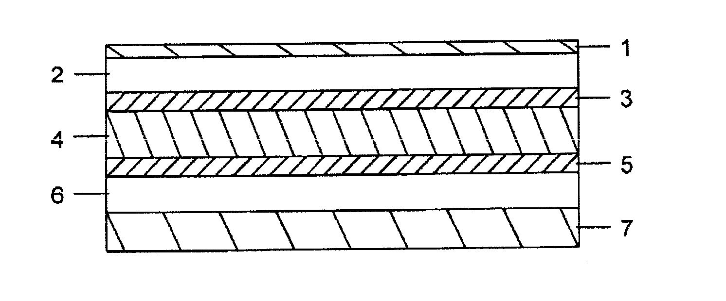
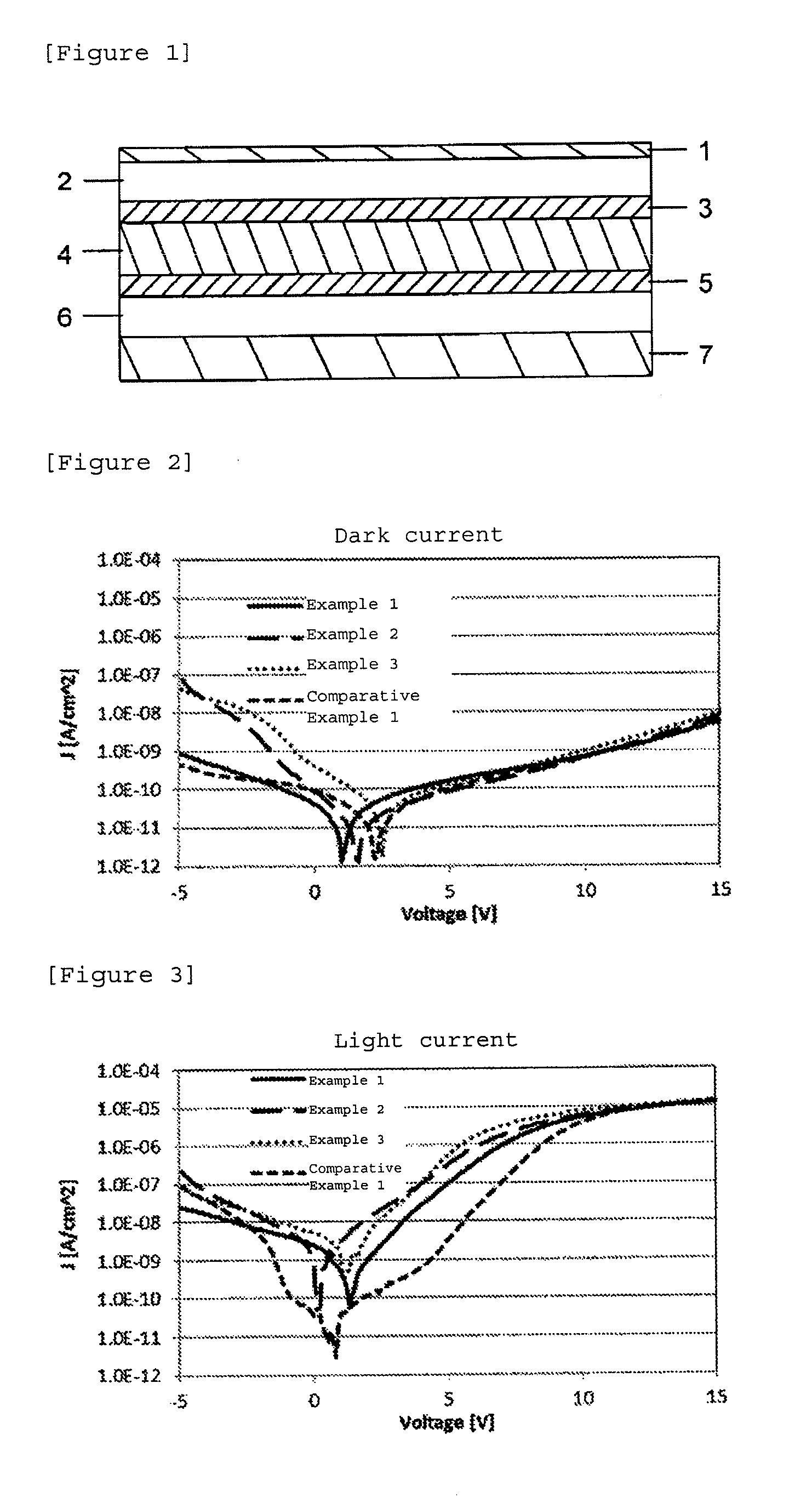
[0072]On ITO transparent conductive glass (manufactured by GEOMATEC Co., Ltd., ITO film thickness: 150 nm), a film of 2,7-diphenyl[1]benzothieno[3,2-b][1]benzothiophene (compound represented by the formula (11) in the specific examples described above) was formed as a blocking layer having a thickness of 50 nm by resistance heating vacuum vapor deposition. Next, on the blocking layer, a film of quinacridone was formed in vacuum as a photoelectric conversion layer having a thickness of 100 nm. Finally, on the photoelectric conversion layer, a film of aluminum was formed in vacuum as an electrode having a thickness of 100 nm to prepare the photoelectric conversion element for use in an imaging element of the present invention. When a voltage of 5 V was applied using the ITO and aluminum electrodes, the current in the dark was −1.68×10⁻¹⁰ A / cm2. When a voltage of 5 V was applied to the transparent conductive glass si...

example 2

Preparation of Photoelectric Conversion Element and Evaluation Thereof

[0073]On ITO transparent conductive glass (manufactured by GEOMATEC Co., Ltd., ITO film thickness: 150 nm), a film of 2,7-bis(4-methylphenyl)[1]benzothieno[3,2-b][1]benzothiophene (compound represented by the formula (14) in the specific examples described above) was formed as a blocking layer having a thickness of 50 nm by resistance heating vacuum vapor deposition. Next, on the blocking layer, a film of quinacridone was formed in vacuum as a photoelectric conversion layer having a thickness of 100 nm. Finally, on the photoelectric conversion layer, a film of aluminum was formed in vacuum as an electrode having a thickness of 100 nm to prepare the photoelectric conversion element for use in an imaging element of the present invention. When a voltage of 5 V was applied using the ITO and aluminum electrodes, the current in the dark was −8.85×10⁻¹¹ A / cm2. When a voltage of 5 V was applied to the transparent conducti...

example 3

Preparation of Photoelectric Conversion Element and Evaluation Thereof

[0074]On ITO transparent conductive glass (manufactured by GEOMATEC Co., Ltd., ITO film thickness: 150 nm), a film of 2,7-bis(4-ethylphenyl)[1]benzothieno[3,2-b][1]benzothiophene (compound represented by the formula (15) in the specific examples described above) was formed as a blocking layer having a thickness of 50 nm by resistance heating vacuum vapor deposition. Next, on the blocking layer, a film of quinacridone was formed in vacuum as a photoelectric conversion layer having a thickness of 100 nm. Finally, on the photoelectric conversion layer, a film of aluminum was formed in vacuum as an electrode having a thickness of 100 nm to prepare the photoelectric conversion element for use in an imaging element of the present invention. When a voltage of 5 V was applied using the ITO and aluminum electrodes, the current in the dark was 1.41×10⁻¹⁰ A / cm2. When a voltage of 5 V was applied to the transparent conductive...


PUM


Abstract

The present invention provides a material for photoelectric conversion elements for use in imaging elements which comprises a compound represented by the following formula (1). The material for photoelectric conversion elements for use in imaging elements, which comprises a compound represented by the following formula (1), is used to produce a photoelectric conversion element which is excellent in terms of hole- or electron-leakage prevention, thermal resistance to processing temperatures, transparency to visible light, etc. (In formula (1), R1 and R2 each independently represent a substituted or unsubstituted aromatic group.)

Description

TECHNICAL FIELD[0001]The present invention relates to a photoelectric conversion element, an imaging element, a photosensor, and a material for a photoelectric conversion element for use in an imaging element which is used for these devices.BACKGROUND ART[0002]In recent years, organic electronic devices have received growing attention. Examples of their features include flexible structures, possible large areas, and inexpensive and high-speed printing methods available in electronic device manufacturing processes. Typical examples of the devices include organic EL elements, organic solar cell elements, organic photoelectric conversion elements, and organic transistor elements. The organic EL elements are expected as main targets for next-generation display purposes as flat panel displays and applied to mobile phone displays, TV, etc. The organic EL elements are still under development with the aim of higher functionalization. Research and development are ongoing as to the organic so...

Claims


Application Information

Patent Timeline
IPC IPC(8): H01L51/00C07D495/04
CPCH01L51/0074H01L51/441H01L27/307C07D495/04H01L27/146Y02E10/549H10K39/32H10K85/6576H10K30/20H10K2102/103H01L31/10H10K30/81
Inventor YAKUSHIJI, HIDENORINIIMI, KAZUKIMORITA, RYOUTAROUYAMAMOTO, TATSUYAINOUCHI, TOSHIFUMIHAMADA, MASAHIRO
Owner NIPPON KAYAKU CO LTD
Why Eureka
Try Eureka