Semiconductor device

a technology of semiconductor devices and semiconductors, applied in semiconductor devices, diodes, electrical devices, etc., can solve the problems of increasing recovery loss, reducing recovery capability, and inability to stop the flow of holes, so as to improve recovery characteristics

Active Publication Date: 2017-03-16
DENSO CORP
View PDF9 Cites 17 Cited by
  • Summary
  • Abstract
  • Description
  • Claims
  • Application Information

AI Technical Summary

Benefits of technology

[0014]As a result, the recovery characteristics can be improved in the a...

Problems solved by technology

However, the aforementioned semiconductor device cannot stop holes flowing into the diode region (diode device) from the IGBT region (IGBT device) at the time of recovery of the diode device.
This causes degradation in the recovery characteristics ...

Method used


Image

  • Semiconductor device
  • Semiconductor device
  • Semiconductor device

Examples


first embodiment

[0038]A first embodiment of the present disclosure will be described. Note that a semiconductor device of the present embodiment is suited for use as a power switching device employed in a power supply circuit such as an inverter or a DC / DC converter.

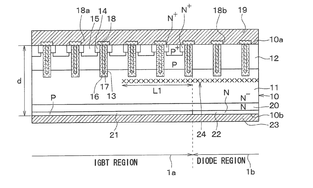
[0039]As illustrated in FIG. 1, the semiconductor device includes a cell region 1 and a periphery region 2 surrounding the cell region 1.

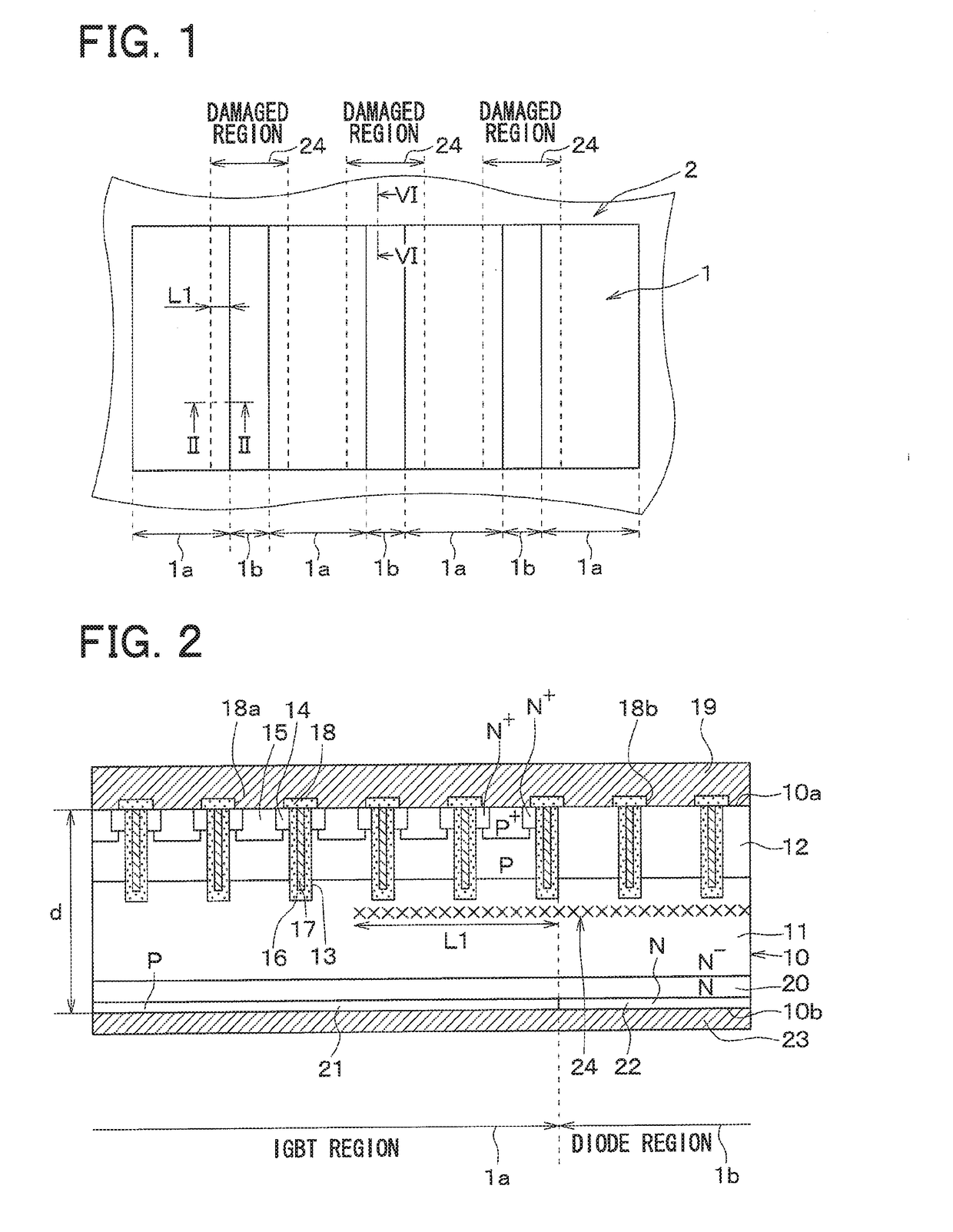
[0040]An IGBT region 1a in which an IGBT device is formed and a diode region 1b in which a diode device is formed are alternately formed in the cell region 1, as illustrated in FIGS. 1 and 2.

[0041]Specifically, the IGBT region 1a and the diode region 1b (cell region 1) are formed on an N−-type semiconductor substrate 10 functioning as a drift layer 11. The IGBT region 1a and the diode region 1b extend along one direction (vertical direction with respect to FIG. 1) of one surface 10a of the semiconductor substrate 10 and are formed alternately in a direction orthogonal to the direction of extension.

[004...

second embodiment

[0077]A second embodiment of the present disclosure will be described. Unlike the first embodiment, a damaged region 24 is also formed in a periphery region 2 in the present embodiment. The rest is similar to the first embodiment and thus will not be described.

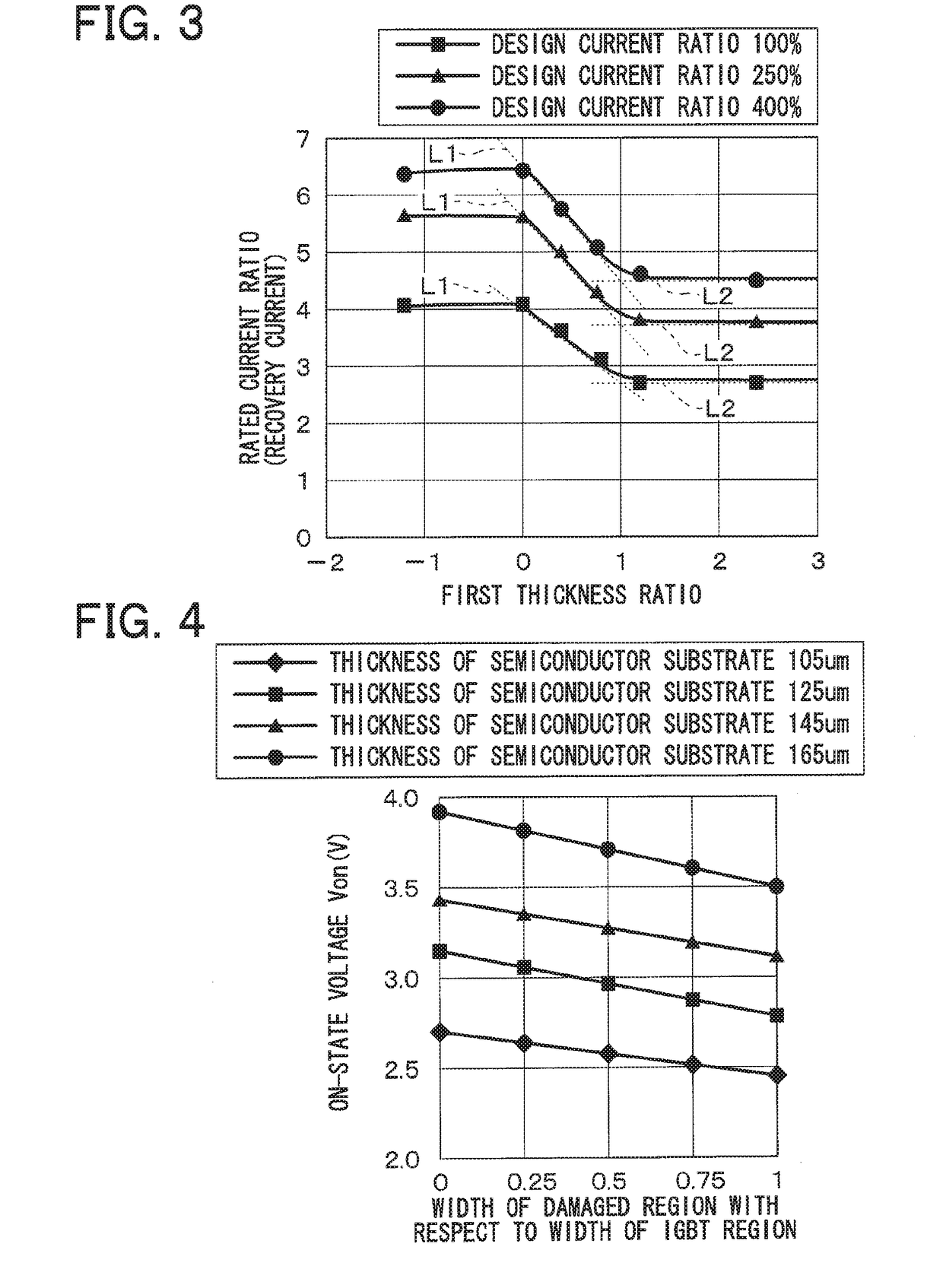
[0078]As illustrated in FIGS. 10 and 11, the damaged region 24 formed in a diode region 1b extends into the periphery region 2 in the present embodiment. As a result, holes (excess carriers) in a drift layer 11 in the periphery region 2 recombine with the damaged region 24 formed in the periphery region 2 and vanish, whereby injection of the holes from the periphery region 2 into the diode region 1b can be prevented.

[0079]The relationship between the damaged region 24 formed in the periphery region 2 and the thickness of a semiconductor substrate 10 will now be described. In the following description, the width of the damaged region 24 formed in the periphery region 2 is denoted as L2, and the width of the damaged region 24 fo...

third embodiment

[0085]A third embodiment of the present disclosure will be described. The shape of a damaged region 24 of the present embodiment is modified from that of the second embodiment. The rest is similar to the first embodiment and thus will not be described.

[0086]In the present embodiment, as illustrated in FIG. 14, the width of the damaged region 24 formed in an IGBT region 1a is larger in an area formed on both end sides of the boundary between a diode region 1b and the IGBT region 1a than in an area formed at the center between both ends. Specifically, the width (length in a horizontal direction with respect to FIG. 14) of the area formed on both end sides of the boundary with the diode region 1b in the IGBT region 1a is denoted as L2.

[0087]As a result, injection of holes from the periphery region 2 into the diode region 1b through the IGBT region 1a can be prevented and, at the same time, recovery characteristics of the diode region 1b can be improved.

[0088]Note that when such a semic...


PUM


Abstract

A semiconductor device includes a semiconductor substrate with: a drift layer; a base layer; and a collector layer and a cathode layer. In the semiconductor substrate, when a region operating as an IGBT device is an IGBT region and a region operating as a diode device is a diode region, the IGBT and diode regions are arranged alternately in a repetitive manner; a damaged region is arranged on a surface portion of the diode region in the semiconductor substrate. The IGBT and diode regions are demarcated by a boundary between the collector and cathode layers; and a surface portion of the IGBT region includes: a portion having the damaged region at a boundary side with the diode region; and another portion without the damaged region arranged closer to an inner periphery side relative to the boundary side.

Description

CROSS REFERENCE TO RELATED APPLICATION[0001]This application is based on Japanese Patent Application No. 2014-61813 filed on Mar. 25, 2014, the disclosure of which is incorporated herein by reference.TECHNICAL FIELD[0002]The present invention relates to a semiconductor device having an IGBT (Insulated Gate Bipolar Transistor) region and a diode (Free Wheeling Diode) region.BACKGROUND ART[0003]There has been proposed a semiconductor device having an IGBT region in which an IGBT device is formed as a switching device used for an inverter or the like, and a diode region in which a diode device is formed (refer to Patent Literature 1, for example).[0004]Specifically, the semiconductor device includes a base layer formed on the surface of a semiconductor substrate making up an N-type drift layer and a trench gate structure passing through the base layer. A P-type collector layer and an N-type cathode layer are formed on the back side of the semiconductor substrate, where an N-type emitte...

Claims


Application Information

Patent Timeline
IPC IPC(8): H01L29/06H01L29/739H01L21/22H01L29/10H01L29/66H01L27/06H01L29/861
CPCH01L29/063H01L27/0664H01L29/7397H01L29/861H01L29/1095H02M7/003H01L29/0638H01L29/66348H01L29/6609H01L21/221H01L29/0696H01L29/32H01L29/8613H01L29/0619H01L29/407H01L27/0727
Inventor KOUNO, KENJI
Owner DENSO CORP
Why Eureka
Try Eureka