
Spin logic device and electronic equipment including same

Active Publication Date: 2017-03-16
INST OF PHYSICS - CHINESE ACAD OF SCI
View PDF1 Cites 30 Cited by
  • Summary
  • Abstract
  • Description
  • Claims
  • Application Information

AI Technical Summary

Benefits of technology

This patent describes a device called a spin logic device which uses a special layer called a spin Hall effect layer to receive logic input currents and a magnetic tunnel junction to process those currents. The device also has a current wiring that works alongside the spin Hall effect layer to pass read currents through the magnetic tunnel junction. The technical effect of this invention is a more efficient and accurate processing of logic inputs, utilizing the spin Hall effect layer in combination with the magnetic tunnel junction.

Problems solved by technology

Unfortunately, the prior art spin logic device 100 of FIG. 1 has several shortcomings.
For example, it contains too many wirings and thus a very complex structure such that the manufacture thereof faces many challenges.
In addition, since the spin logic device 100 relies completely on the Oersted field generated by a current passing through the input lines to reverse magnetization of the ferromagnetic layers, it has to use a large current in order to generate an Oersted field strong enough to reverse the magnetization, leading to high power consumption.
These shortcomings have obstructed the practical application of the prior art spin logic devices in modern electronics equipments.

Method used


Image

  • Spin logic device and electronic equipment including same
  • Spin logic device and electronic equipment including same
  • Spin logic device and electronic equipment including same

Examples


Embodiment Construction

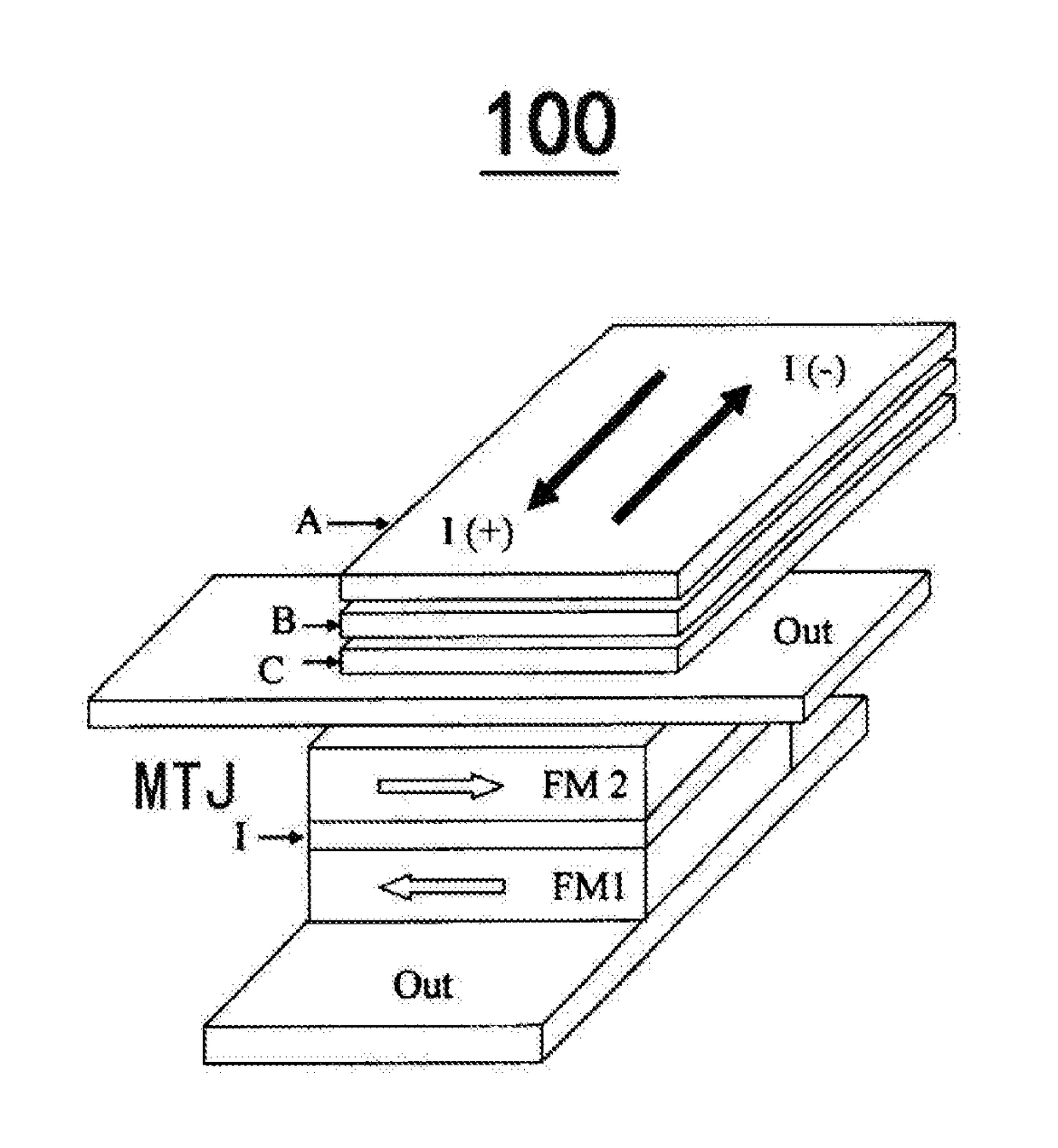
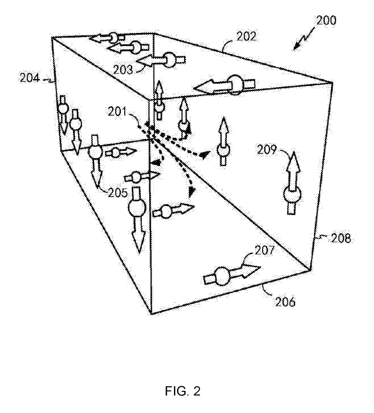
[0019]FIG. 2 is a schematic diagram displaying the Spin Hall effect. Referring to FIG. 2, while flowing through a particular conductor 200, electrons 201 are spin-polarized on surfaces 202, 204, 206, and 208 of the conductor 200 due to spin-orbit coupling, as shown by arrows 203, 205, 207, and 209, respectively. This phenomenon is known as Spin Hall effect. Examples of materials exhibiting Spin Hall effect include, but not limited to metals or alloys such as Pt, Au, Ta, Pd, Ir, W, Bi, Pb, Hf, IrMn, PtMn, AuMn, topological insulators such as Bi2Se3 and Bi2Te3, and rare earth materials such as Y, La, Ce, Pr, Nd, Sm, Eu, Gd, Te, Dy, Ho, Er, Tm, Yi, Lu, among which Y, Nd, Sm, Eu, Gd, Te, Dy, Ho, Er and Tm are preferable as they have stronger spin-orbit coupling and hence a larger Spin Hall angle. It is also known that for different Spin Hall effect materials, the spin polarization of electrons may be in opposite directions even when the current is applied in the same direction.

[0020]The...


PUM


Abstract

The present invention relates to a spin logic device and an electronic equipment comprising the same. A spin logic device may include a Spin Hall effect (SHE) layer formed of a conductive material having Spin Hall effect and configured to receive a first logic input current and a second logic input current, the first logic input current and the second logic input current both being an in-plane current, a magnetic tunnel junction provided on the SHE layer comprising a free magnetic layer in contact with the SHE layer, a barrier layer disposed on the free magnetic layer, and a reference magnetic layer disposed on the barrier layer, and a current wiring in connection to the reference magnetic layer side of the magnetic tunnel junction, the current wiring being in cooperation with the SHE layer to apply a read current passing through the magnetic tunnel junction therebetween.

Description

CROSS-REFERENCE TO RELATED APPLICATIONS[0001]This application claims priority to Chinese Patent Application No. 201510574526.5 entitled “Current-Driving Magnetic Random Access Memory and Spin Logic Device” filed on Sep. 10, 2015, Chinese Patent Application No. 201610064129.8 entitled “Spin Logic Device and Electronic Equipment Including Same” filed on Jan. 29, 2016, and Chinese Patent Application No. 201610190767.4 entitled “Programmable Spin Logic Device and Electronic Equipment Including Same” filed on Mar. 30, 2016, the disclosures of which are incorporated herein by reference in their entireties.FIELD OF THE INVENTION[0002]The present invention generally relates to spintronics, and in particular, to a spin logic device utilizing Spin Hall effect and an electronic equipment including the spin logic device.BACKGROUND[0003]Spin logic device, also known as magnetic logic device, is a kind of logic device that is formed with magnetic materials and operates by using electron spin char...

Claims


Application Information

Patent Timeline
IPC IPC(8): H01L43/06H01L27/22H01L43/08H01L43/10H01L43/04G11C11/16
CPCH01L43/065H01L43/04H01L27/222H01L43/08H01L43/10G11C11/1673G11C11/1659G11C11/18H03K19/18G11C11/1675H10N50/10H10B61/00H10N52/101H10N50/85H10N52/80
Inventor HAN, XIUFENGWAN, CAIHUAZHANG, XUAN
Owner INST OF PHYSICS - CHINESE ACAD OF SCI
Learn More