Spin Hall effect-assisted writing multi-state magnetic random access memory bit and spin Hall effect-assisted writing method
A technology of random access memory and spin Hall effect, applied in the field of non-volatile memory and semiconductor, can solve the problems of adverse effects of chip speed and stability, unfavorable practical application, high manufacturing cost, and achieve fast reading speed. , The effect of reducing write power consumption and improving data storage density
- Summary
- Abstract
- Description
- Claims
- Application Information
AI Technical Summary
Problems solved by technology
Method used
Image
Examples
Embodiment 1
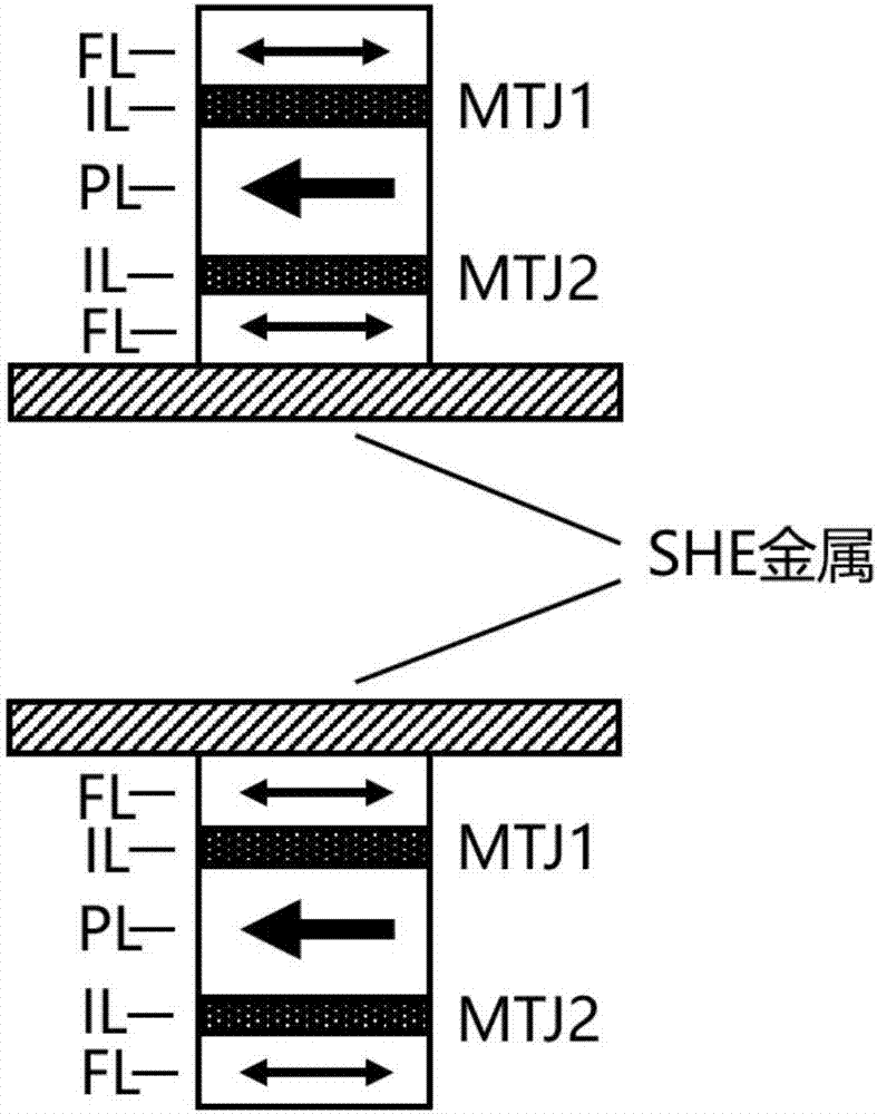
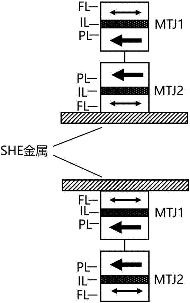
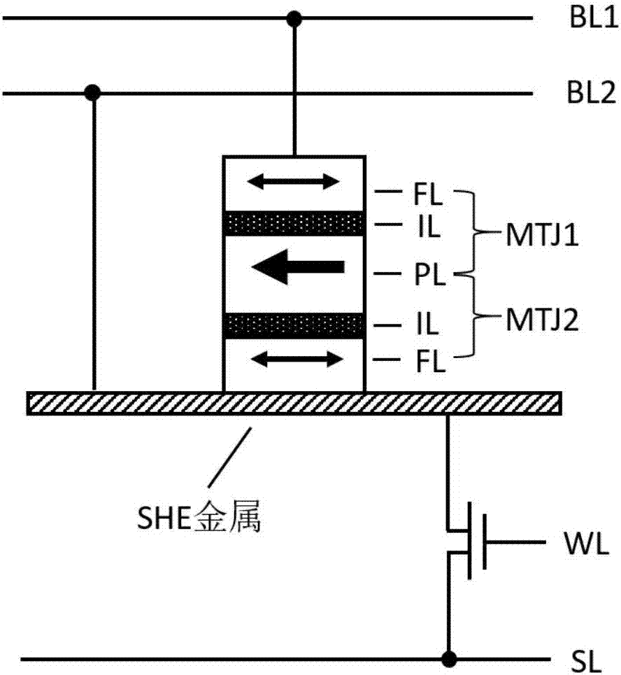
[0023] Example 1: figure 1 , figure 2 The reference signs of are: free magnetic layer FL, pinned magnetic layer PL, insulating layer IL, magnetic tunnel junction MTJ; image 3 with Figure 4 Reference numerals are: word line WL, bit line BL, source line SL, magnetic tunnel junction MTJ, CMOS transistor.
[0024] This embodiment is a spin Hall effect assisted STT-MRAM multi-state memory cell with a double bit line structure. In this embodiment, the basic structure of the multi-state memory cell assisted by the spin Hall effect of the double bit line structure is as follows image 3 As shown, it includes a word line WL, two bit lines BL1 and BL2, a source line SL, an in-plane multi-state magnetic storage bit, and a memory cell selection switch composed of CMOS transistors. Among them, the structure of the in-plane multi-state magnetic storage bit is as follows figure 1 , figure 2 As shown, it includes an in-plane magnetic tunnel junction MTJ1 and an in-plane magnetic tun...
Embodiment 2
[0029] Embodiment 2: This embodiment is a spin Hall effect assisted STT-MRAM multi-state memory cell with a double CMOS transistor structure. In this embodiment, the basic structure of the STT-MRAM multi-state memory cell assisted by the spin Hall effect of the dual CMOS transistor structure is as follows Figure 4 As shown, it includes a bit line BL, an in-plane multi-state magnetic storage bit, a memory cell selection switch composed of two CMOS transistors, its source lines SL1 and SL2, and word lines WL1 and WL2. Among them, the structure of the in-plane multi-state magnetic storage bit is as follows figure 1 , figure 2 As shown, it includes an in-plane magnetic tunnel junction MTJ1 and an in-plane magnetic tunnel junction MTJ2, and each MTJ is composed of a free magnetic layer FL, a pinned magnetic layer PL, and an insulating layer IL. Among them, the magnetization directions of the magnetic layers of MTJ1 and MTJ2 are located in the film plane, and the positions of th...
PUM
 Abstract
Description
Claims
Application Information


