
Bidirectional spin Hall effect-based magnetic non-volatile memory unit structure

A spin Hall effect, non-volatile storage technology, applied in the field of memory, can solve the problems of low polarizability, weakened memory cell stability, high write power consumption, etc., to reduce write power consumption and shorten write power. The effect of entering the operating time

Active Publication Date: 2017-11-03
TAIYUAN UNIV OF TECH
View PDF4 Cites 15 Cited by
  • Summary
  • Abstract
  • Description
  • Claims
  • Application Information

AI Technical Summary

Problems solved by technology

The auxiliary scheme based on the external magnetic field will weaken the stability of the memory cell and limit the storage density of SHE-MRAM to a certain extent
The STT-based auxiliary scheme requires relatively complex peripheral circuits to achieve precise coordination of multiple write electrical pulses. At the same time, this scheme may cause breakdown of the magnetic tunnel junction insulating layer, resulting in damage to the memory cell.
In addition, the previous SHE-MRAM only used the unidirectional polarization current generated by the spin Hall effect, resulting in low polarizability and high write power consumption.

Method used

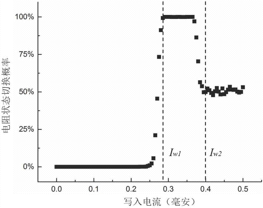
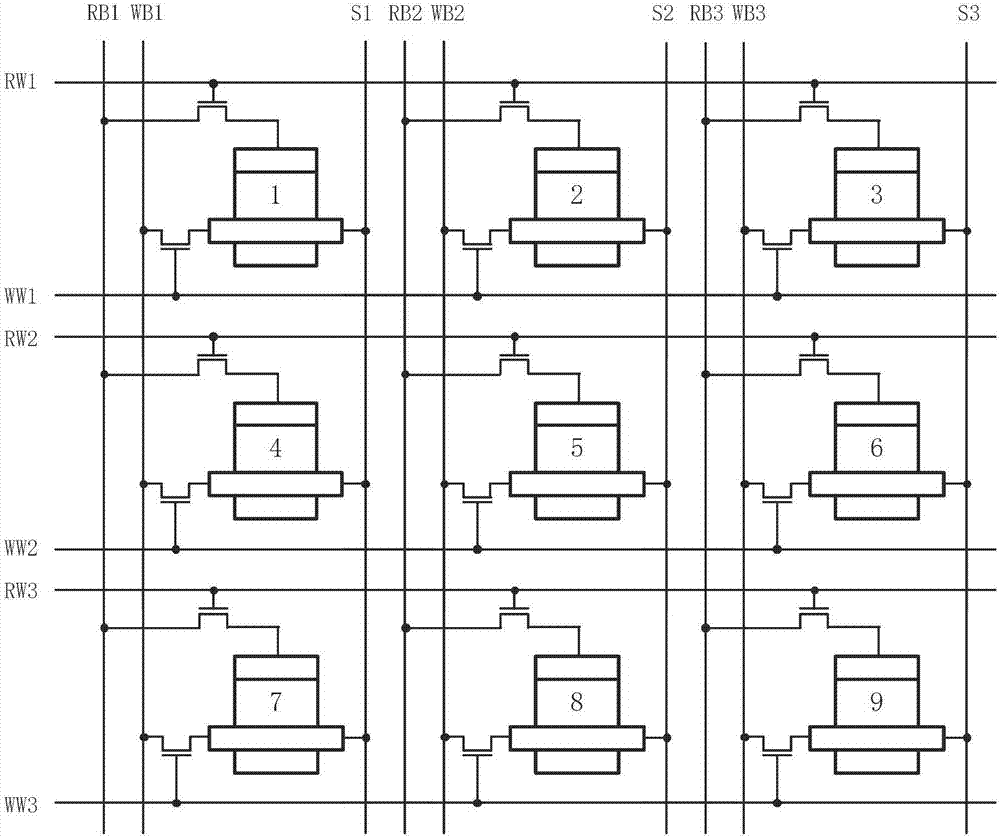

Image

  • Bidirectional spin Hall effect-based magnetic non-volatile memory unit structure
  • Bidirectional spin Hall effect-based magnetic non-volatile memory unit structure
  • Bidirectional spin Hall effect-based magnetic non-volatile memory unit structure

Examples


Embodiment Construction

[0023] In order to make the purpose, technical solutions and advantages of the embodiments of the present invention clearer, the technical solutions in the embodiments of the present invention will be clearly and completely described below in conjunction with the drawings in the embodiments of the present invention. Obviously, the described embodiments It is a part of embodiments of the present invention, but not all embodiments.

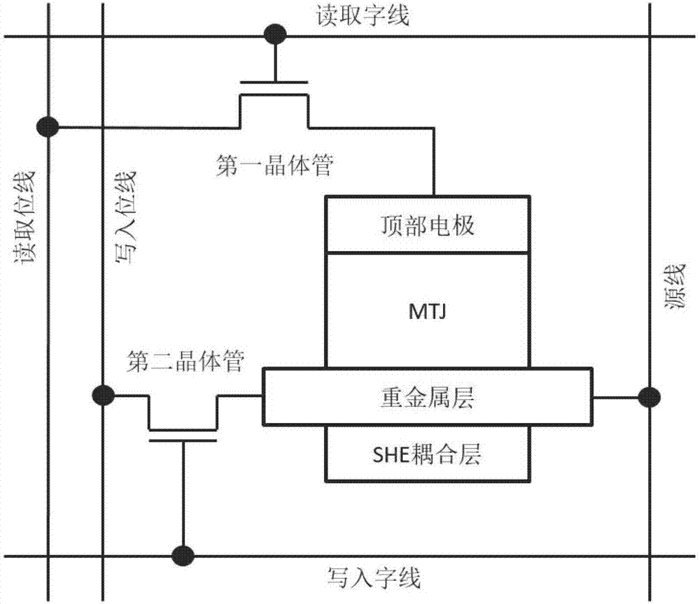
[0024] figure 1 It is a schematic diagram of the circuit structure of the SHE-MRAM storage unit of the present invention; as figure 1 As shown, the present invention provides a magnetic nonvolatile memory unit based on the bidirectional spin Hall effect, comprising: a bidirectional spin Hall effect magnetic tunnel junction, a first transistor, a second transistor, a read word line, a read A bit line, a write word line, a write bit line and a source line; wherein, the gate of the first transistor is connected to the read word line, and the source of...


PUM

PropertyMeasurementUnit
Thicknessaaaaaaaaaa
Thicknessaaaaaaaaaa
Thicknessaaaaaaaaaa

Abstract

The invention discloses a bidirectional spin Hall effect-based magnetic non-volatile memory unit structure. The bidirectional spin Hall effect-based magnetic non-volatile memory unit structure comprises a bidirectional spin Hall effect magnetic tunneling junction, a first transistor, a second transistor, a reading word line, a reading bit line, a writing word line, a writing bit line and a source line, wherein the bidirectional spin Hall effect-based novel magnetic tunneling junction comprises a traditional vertical magnetic tunneling junction, a heavy metal layer and a spin Hall effect coupling layer, the vertical magnetic tunneling junction comprises a reference layer, a tunneling insulation layer and a first magnetic free layer from top to bottom, and the spin Hall effect coupling layer comprises a second magnetic free layer and an insulation layer from top to bottom. By the bidirectional spin Hall effect-based magnetic non-volatile memory unit structure, an auxiliary means is not needed, the switching of the resistance of the vertical magnetic tunneling junction among a high-resistance state, a low-resistance state and a random-resistance state is achieved only by controlling a current passing through the heavy metal layer, the writing power consumption of the magnetic memory unit can be effectively reduced, and the writing operation time of the magnetic memory unit is shortened.

Description

technical field [0001] The invention relates to the field of memory, in particular to a magnetic non-volatile memory unit structure based on the bidirectional spin Hall effect. Background technique [0002] Both traditional SRAM and DRAM are volatile memories, which require continuous power supply during their working process. With the development of manufacturing process, the problem of power consumption caused by leakage and refresh current is becoming more and more serious, which limits the further improvement of memory performance to a large extent. In recent years, a variety of non-volatile storage schemes, such as phase-change storage, resistive-change storage, conductive bridge storage, magnetic storage, etc., have developed rapidly, and are expected to replace the storage mode based on traditional transistors and capacitors and become the next generation of non-von Neuy An integral part of the Man computer architecture. Among them, the magnetic memory based on the ...

Claims


Application Information

Patent Timeline
IPC IPC(8): H01L43/06
CPCH10N52/101
Inventor 李晓光冯秀芳刘喆颉
Owner TAIYUAN UNIV OF TECH
Learn More