A magnetic tunnel junction with strong perpendicular magnetic anisotropy

A magnetic tunnel junction, anisotropic technology, applied in the fields of non-volatile magnetic memory and magnetic logic, can solve the problems of large magnetic damping coefficient, low spin transfer torque reversal efficiency, and increased film complexity.

Active Publication Date: 2020-07-07
BEIHANG UNIV
View PDF5 Cites 0 Cited by
  • Summary
  • Abstract
  • Description
  • Claims
  • Application Information

AI Technical Summary

Problems solved by technology

When the thermal stability factor drops below 60, it generally cannot meet the requirements for long-term reliable storage of data
Secondly, due to the weak interface perpendicular magnetic anisotropy, in order to maintain sufficient thermal stability (for example, the thermal stability coefficient is greater than 60), the cross-sectional size of the magnetic tunnel junction is required to be large and the thickness of the free layer is small, such as Figure 2B , resulting in a lower storage density of the MRAM
In addition, the smaller thickness of the free layer results in a larger magnetic damping coefficient and lower spin-transfer torque reversal efficiency
Finally, due to the weak interfacial perpendicular magnetic anisotropy, a double-interface structure is required to enhance the perpendicular magnetic anisotropy of the free layer, and usually a structure such as a Co / Pt multilayer film is required to enhance the perpendicular magnetic anisotropy of the reference layer , thereby increasing the number of film layers in the magnetic tunnel junction, thus increasing the complexity of film growth during the preparation of the magnetic tunnel junction

Method used


Image

  • A magnetic tunnel junction with strong perpendicular magnetic anisotropy
  • A magnetic tunnel junction with strong perpendicular magnetic anisotropy
  • A magnetic tunnel junction with strong perpendicular magnetic anisotropy

Examples


Embodiment 1

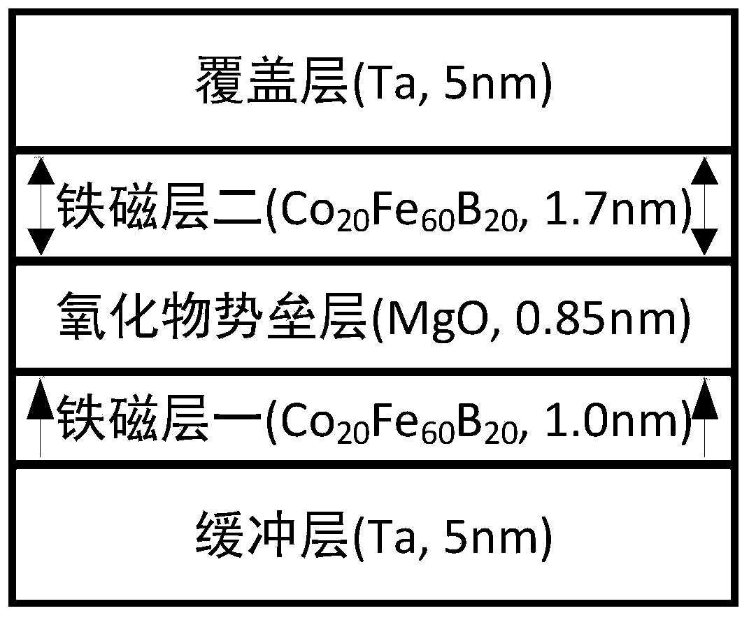
[0042] In this embodiment, the buffer layer, the ferromagnetic layer 1, the barrier layer, the ferromagnetic layer 2 and the cover layer are deposited on the thermally oxidized silicon substrate in the order from bottom to top by magnetron sputtering, such as Figure 4A shown. Among them, the material of the buffer layer is Ta, the thickness is 5nm; the material of the ferromagnetic layer is Co 20 Fe 60 B 20 , the thickness is 20nm; the material of the barrier layer is MgO, the thickness is 1nm; the material of the ferromagnetic layer 2 is Co 20 Fe 60 B 20 , with a thickness of 30nm; the material of the covering layer is Ta, with a thickness of 5nm. Finally, processing such as photolithography and etching is performed, and the cross-sectional shape is circular with a diameter of 10 nm. The buffer layer can have functions such as reducing surface roughness and promoting the formation of the growth crystal direction of the multilayer film, and the covering layer can have f...

Embodiment 2

[0048] In this embodiment, the buffer layer, the ferromagnetic layer 1, the barrier layer, the ferromagnetic layer 2 and the cover layer are deposited on the thermally oxidized silicon substrate in the order from bottom to top by magnetron sputtering, such as Figure 4B shown. Among them, the material of the buffer layer is Ta, the thickness is 5nm; the material of the ferromagnetic layer is Co 20 Fe 60 B 20 , the thickness is 30nm; the material of the barrier layer is MgO, the thickness is 1nm; the material of the ferromagnetic layer 2 is Co 20 Fe 60 B 20, with a thickness of 20nm; the material of the covering layer is Ta, with a thickness of 5nm. Finally, processing such as photolithography and etching is performed, and the cross-sectional shape is circular with a diameter of 10 nm. The buffer layer can have functions such as reducing surface roughness and promoting the formation of the growth crystal direction of the multilayer film, and the covering layer can have fu...

Embodiment 3

[0054] In this embodiment, the buffer layer, the ferromagnetic layer 1, the barrier layer, the ferromagnetic layer 2 and the covering layer are deposited on the thermally oxidized silicon substrate in sequence from bottom to top by magnetron sputtering. Wherein, the material of buffer layer is W, and the thickness is 8nm; The material of ferromagnetic layer 1 is Co 40 Fe 40 B 20 , the thickness is 100nm; the material of barrier layer is MgO, the thickness is 1.5nm; the material of ferromagnetic layer 2 is Co 40 Fe 40 B 20 , with a thickness of 120nm; the material of the covering layer is W, with a thickness of 5nm. Finally, photolithography, etching and other processing are performed, and the cross-sectional shape is circular with a diameter of 1nm. The buffer layer can have functions such as reducing surface roughness and promoting the growth crystal orientation of the multilayer film, and the covering layer can have functions such as anti-oxidation and reducing surface ...


PUM

PropertyMeasurementUnit
sizeaaaaaaaaaa
thicknessaaaaaaaaaa
thicknessaaaaaaaaaa

Abstract

The present invention is a magnetic tunnel junction with strong perpendicular magnetic anisotropy, its structure is ferromagnetic layer 1, potential barrier layer, and ferromagnetic layer 2 from bottom to top; it is characterized in that: the cross-sectional size of the magnetic tunnel junction is in Between 1nm and 150nm, the thickness of ferromagnetic layer 1 and ferromagnetic layer 2 is greater than 6nm, and the thickness of ferromagnetic layer 1 and ferromagnetic layer 2 is greater than half of the cross-sectional size; the thickness of the barrier layer is 0.2‑10nm . Compared with the existing technology, the device has the advantages of strong perpendicular magnetic anisotropy, high thermal stability, small cross-sectional size, high spin-transfer torque reversal efficiency, and fewer film layers.

Description

【Technical field】 [0001] The invention relates to a magnetic tunnel junction with strong perpendicular magnetic anisotropy, which belongs to the technical field of nonvolatile magnetic memory and magnetic logic. 【Background technique】 [0002] Magnetic random access memory (MRAM) and magnetic logic have the advantages of non-volatility, fast read and write speed, low power consumption, unlimited erasing and writing, etc., and have attracted extensive attention from industry and academia. [0003] The core device of magnetic random access memory and magnetic logic is the magnetic tunnel junction (Magnetic Tunnel Junction, MTJ). The basic structure of the magnetic tunnel junction consists of three thin films: ferromagnetic layer, barrier layer, and ferromagnetic layer. When the magnetization directions of the two ferromagnetic layers are the same, the resistance of the structure is low; when the magnetization directions of the two ferromagnetic layers are opposite, the resist...

Claims


Application Information

Patent Timeline
Patent Type & Authority Patents(China)
IPC IPC(8): H01L43/08
CPCH10N50/10
Inventor 赵巍胜彭守仲康旺张有光
Owner BEIHANG UNIV
Why Eureka
Try Eureka