Integrated circuit with replacement gate stacks and method of forming same

a technology of integrated circuits and gate stacks, which is applied in the field of gate stacks, can solve the problems of reducing the drain current and transconductance of the integrated circuit, increasing the threshold voltage, and chlorine (cl) and fluorine (f) are not compatible to improve the nbti simultaneously

Active Publication Date: 2017-04-20
IBM CORP
View PDF4 Cites 28 Cited by
  • Summary
  • Abstract
  • Description
  • Claims
  • Application Information

AI Technical Summary

Benefits of technology

[0006]A first aspect of the invention provides for a method of forming a replacement gate stack for a p-type field-effect transistor (pFET) and an n-type field-effect transistor (nFET). The method may include: forming an interfacial layer in a first opening in a pFET region and a second opening in an nFET region, each opening being in a dielectric layer in the pFET region and the nFET region; forming a high-k layer over the interfacial layer in each of the first and second openings; forming a wetting layer over the high-k layer in each of the first and second openings; forming a first metal layer in each of the first and second openings, the first metal layer including tungsten; and forming a first gate electrode layer over the first metal layer to substantially fill each of the first and second openings, thereby forming a first replacement gate stack over the pFET region and a second replacement gate stack over the nFET region.
[0007]A second aspect of the invention provides for an integrated circuit (IC) structure. The IC structure may include: a first replacement gate stack in a dielectric layer in a pFET region, the first replacement gate stack including: an interfacial layer in a first opening in the dielectric layer; a high-k layer over the interfacial layer in the first opening; a wetting layer over the high-k layer in the first opening; a first metal layer over the wetting layer in the first opening, the first metal layer including tungsten; and a first gate electrode layer over the first metal layer and substantially filling the first opening; and a second replacement gate stack in the dielectric layer in an nFET region, the second gate stack being laterally adjacent to the first gate stack and including: the interfacial layer in a second opening in the dielectric layer; the high-k layer over the interfacial layer in the second opening; a first gate electrode layer over the high-k layer and substantially filling the second opening.

Problems solved by technology

One challenge associated with RMG processing is reducing gate resistance in a p-type field-effect transistor without affecting the gate resistance in an n-type field-effect transistor or work function metals used to form the gates.
NBTI is a reliability issue which results in an increase in the threshold voltage and a decrease in both the drain current and transconductance of the integrated circuit when the NBTI is poor.
However, chlorine (Cl) and fluorine (F) are not compatible to simultaneously improve the NBTI.
However, this increases the thickness of the inversion layer, or the area under the gate, which in turn reduces capacitance.

Method used


Image

  • Integrated circuit with replacement gate stacks and method of forming same
  • Integrated circuit with replacement gate stacks and method of forming same
  • Integrated circuit with replacement gate stacks and method of forming same

Examples


Embodiment Construction

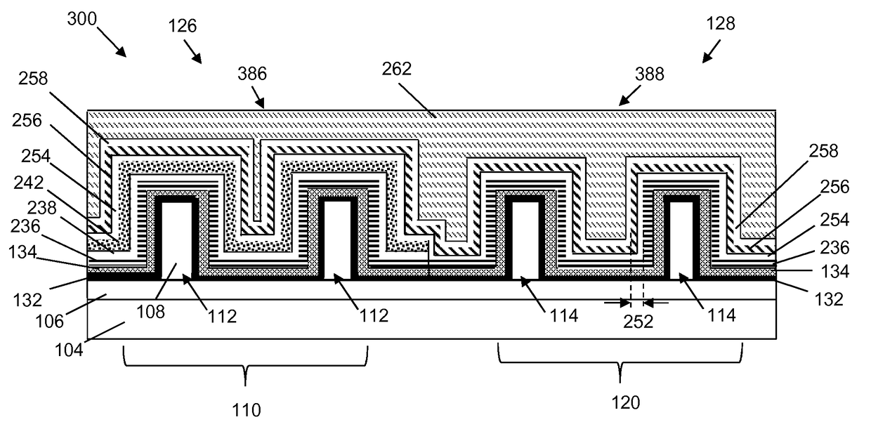
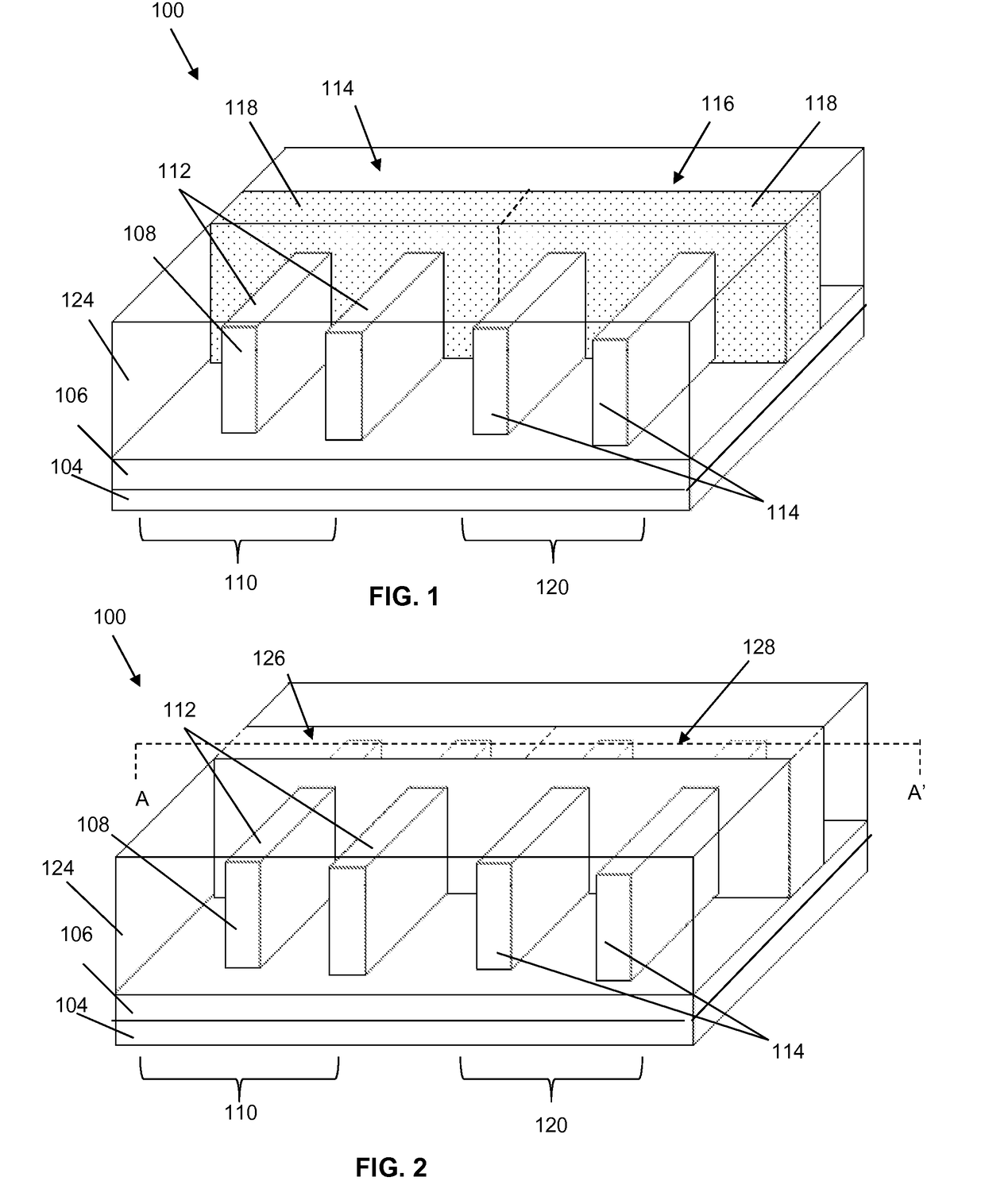
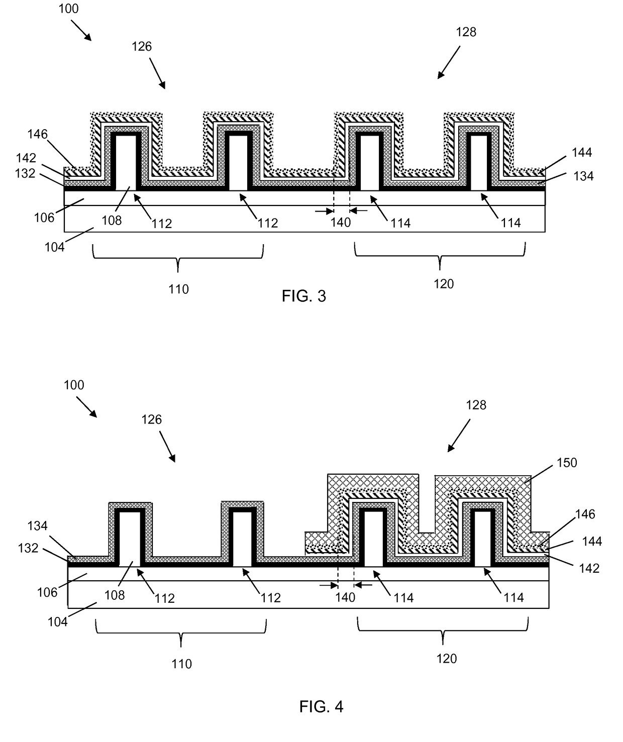
[0013]Aspects of the present disclosure are directed to gate stacks, and more particularly, to replacement gate stacks for p-type field-effect transistors and n-type field effect transistors and methods of forming the same. Specifically, the gate stacks of the present disclosure includes using at least one of a chlorine (Cl)-doped tungsten and a pure tungsten (W) as precursor for a gate electrode. Therefore, the present invention does not include the use of fluorine (F) as a precursor for a gate electrode thereby improving the gate resistance, the negative bias temperature instability (NBTI), and the performance of the integrated circuit.

[0014]Aspects of the present invention are shown and described with respect to a fin-shaped field-effect transistor (FINFET). However, it is to be understood that aspects of the present invention are equally applicable to other types of transistors, such as planar transistors.

[0015]FIG. 1 shows an IC structure as a FINFET 100 that has undergone prel...


PUM

PropertyMeasurementUnit
thicknessaaaaaaaaaa
wettingaaaaaaaaaa
currentaaaaaaaaaa

Abstract

A first aspect of the invention provides for a method including: forming an interfacial layer in a first opening in a pFET region and a second opening in an nFET region, each opening being in a dielectric layer in the pFET region and the nFET region; forming a high-k layer over the interfacial layer in each of the first and second openings; forming a wetting layer over the high-k layer in each of the first and second openings; forming a first metal layer in each of the first and second openings, the first metal layer including tungsten; and forming a first gate electrode layer over the first metal layer to substantially fill each of the first and second openings, thereby forming a first replacement gate stack over the pFET region and a second replacement gate stack over the nFET region.

Description

BACKGROUND[0001]Technical Field[0002]The present invention relates to gate stacks, and more particularly, to replacement gate stacks for p-type field-effect transistors and n-type field effect transistors and methods of forming the same.[0003]Related Art[0004]During integrated circuit fabrication, transistors can be formed in a semiconductor substrate. Each transistor includes a gate through which a current can be passed between source and drain terminals of the transistor. One approach to forming gates includes replacement metal gate (RMG) processing. RMG processing includes generating a number of sacrificial or dummy gates over a structure, such as a fin for a fin field effect transistor (FINFET), so that other processing steps, such as adjacent contact creation, can be carried out without damaging the gate. Once the other processing is carried out, the dummy gates are replaced with a metal to create the final metal gate structure. One challenge associated with RMG processing is r...

Claims


Application Information

Patent Timeline
Patent Type & Authority Applications(United States)
IPC IPC(8): H01L21/8238H01L27/092
CPCH01L21/823842H01L21/823821H01L27/0924H01L21/845H01L27/092
Inventor BAO, RUQIANGKRISHNAN, SIDDARTH A.
Owner IBM CORP
Why Eureka
Try Eureka