Method and system for forming patterns using shaped beam lithography including temperature effects

Active Publication Date: 2017-05-04
D2S
View PDF2 Cites 9 Cited by
  • Summary
  • Abstract
  • Description
  • Claims
  • Application Information

AI Technical Summary

Benefits of technology

The present patent provides methods and systems for delivering multiple shot groups of charged particles to a surface during an overall time period. The methods involve delivering a first shot group onto the surface at a first time period and measuring the temperature influence of secondary effects from a second shot group at another time period. The resulting temperature data is used to determine an effective temperature for the surface and modify the first shot group accordingly. This allows for precise control over the temperature influence during the exposure process. The technical effects of this patent include improved accuracy and control over temperature effects during charged particle beam writing.

Problems solved by technology

An example of an end-use limitation is defining the geometry of a transistor in a way in which it cannot sufficiently operate at the required supply voltage.
The design rule limitations reflect, among other things, the smallest dimensions that can be reliably fabricated.

Method used


Image

  • Method and system for forming patterns using shaped beam lithography including temperature effects
  • Method and system for forming patterns using shaped beam lithography including temperature effects
  • Method and system for forming patterns using shaped beam lithography including temperature effects

Examples


Embodiment Construction

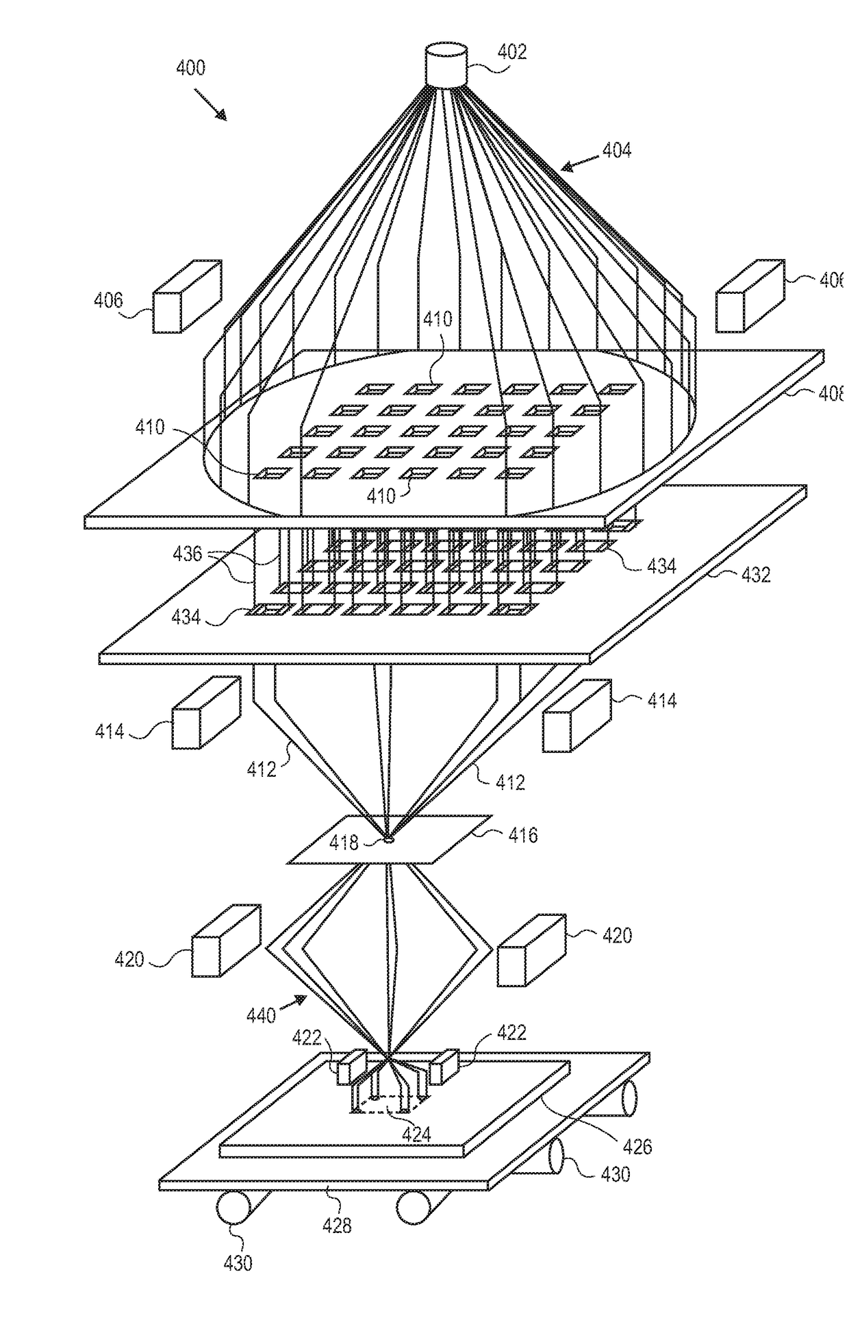
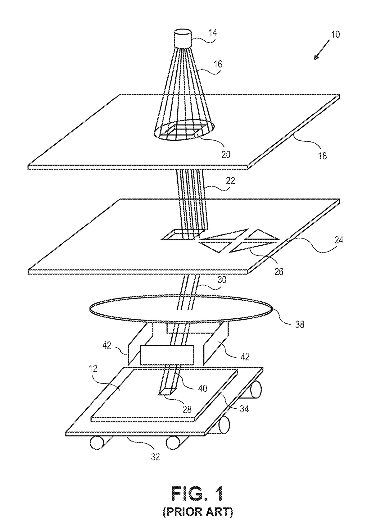
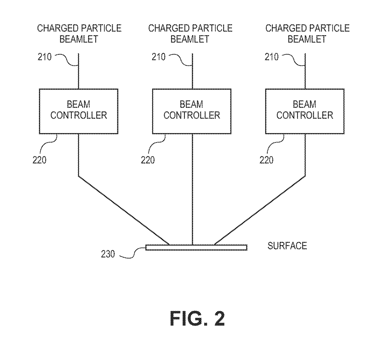
[0027]The present disclosure is related to lithography, and more particularly to the design and manufacture of a surface which may be the surface of a reticle, a wafer, or any other surface, using charged particle beam lithography. Although embodiments shall be described in terms of a semiconductor wafer or a photomask, the methods and systems described herein can also be applied to other components used in the manufacturing of semiconductor devices. The embodiments may also be applied to the manufacturing of various electronic devices such as flat panel displays, micro-electromechanical systems, and other microscopic structures that require precision by electron beam writing. Accordingly, a reference to shots being delivered onto a surface shall apply to, for example, a surface of a semiconductor wafer, or a surface of a reticle or photomask.

[0028]As the size of shapes that are to be formed on a surface such as a reticle decreases in newer fabrication technologies, higher precision...


PUM


Abstract

In some embodiments, data is received defining a plurality of shot groups that will be delivered by a charged particle beam writer during an overall time period, where a first shot group will be delivered onto a first designated area at a first time period. A temperature of the first designated area at a different time period is determined. In some embodiments, the different time period is when secondary effects of exposure from a second shot group are received at the first designated area. In some embodiments, transient temperatures of a target designated area are determined at time periods when exposure from a shot group is received. An effective temperature of the target area is determined, using the transient temperatures and applying a compensation factor based on an amount of exposure received during that time period. A shot in the target shot group is modified based on the effective temperature.

Description

RELATED APPLICATIONS[0001]This application claims priority to U.S. Provisional Patent Application No. 62 / 250,913, entitled “Method and System for Forming Patterns Using Shaped Beam Lithography Including Temperature Effects” and filed on Nov. 4, 2015, which is hereby incorporated by reference for all purposes.BACKGROUND OF THE DISCLOSURE[0002]In the production or manufacturing of semiconductor devices, such as integrated circuits, optical lithography may be used to fabricate the semiconductor devices. Optical lithography is a printing process in which a lithographic mask or photomask or reticle is used to transfer patterns to a substrate such as a semiconductor or silicon wafer to create the integrated circuit (I.C.). Other substrates could include flat panel displays, holographic masks or even other reticles. While conventional optical lithography uses a light source having a wavelength of 193 nm, extreme ultraviolet (EUV) or X-ray lithography are also considered types of optical li...

Claims


Application Information

Patent Timeline
IPC IPC(8): G06F17/50G03F1/36
CPCG03F1/36G06F17/5081H01J37/3026H01J37/3174H01J2237/31771H01J2237/31774G06F30/398
Inventor FUJIMURA, AKIRAZABLE, HAROLD ROBERTPEARMAN, RYANGUTHRIE, WILLIAM
Owner D2S
Why Eureka
Try Eureka