Silicon carbide semiconductor element and method for manufacturing the same

Active Publication Date: 2017-05-04
PANASONIC INTELLECTUAL PROPERTY MANAGEMENT CO LTD
View PDF1 Cites 3 Cited by
  • Summary
  • Abstract
  • Description
  • Claims
  • Application Information

AI Technical Summary

Benefits of technology

The present patent aims to solve two problems faced by vertical SiC-MOSFETs: conduction loss and switching loss. A high-concentration n-type epitaxial layer is formed to reduce conduction loss, but it also increases gate-drain capacitance, which negatively affects switching loss. The present disclosure proposes a configuration that reduces both conduction loss and switching loss by reducing gate-drain capacitance without increasing gate resistance.

Problems solved by technology

Among these various capacitive components, in particular, feedback capacitance, that is, gate-drain capacitance, most largely contributes to switching loss.

Method used


Image

  • Silicon carbide semiconductor element and method for manufacturing the same
  • Silicon carbide semiconductor element and method for manufacturing the same
  • Silicon carbide semiconductor element and method for manufacturing the same

Examples


second exemplary embodiment

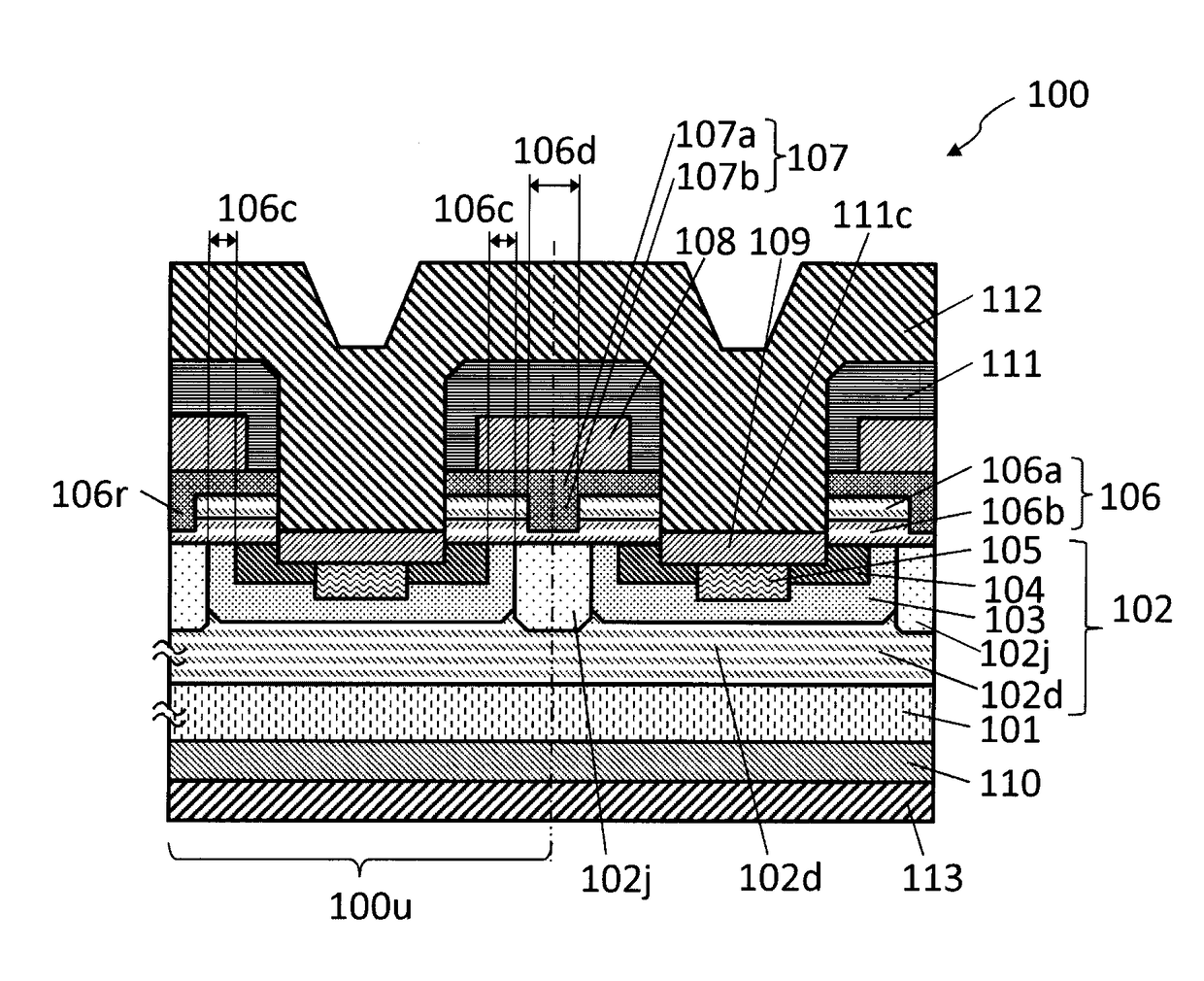
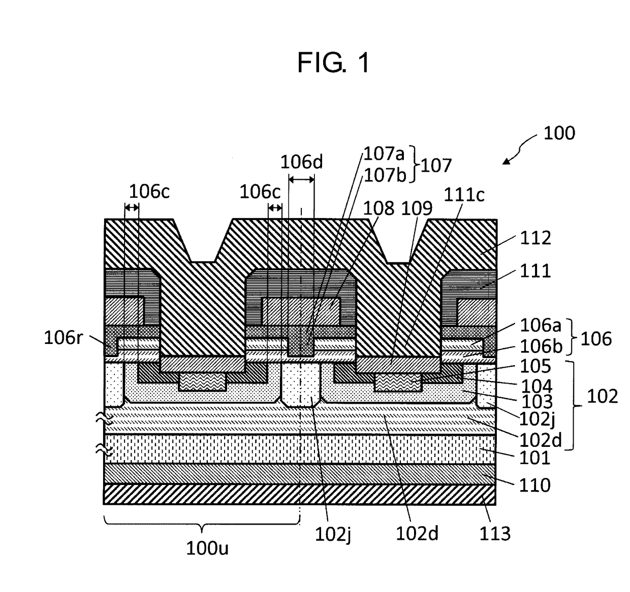
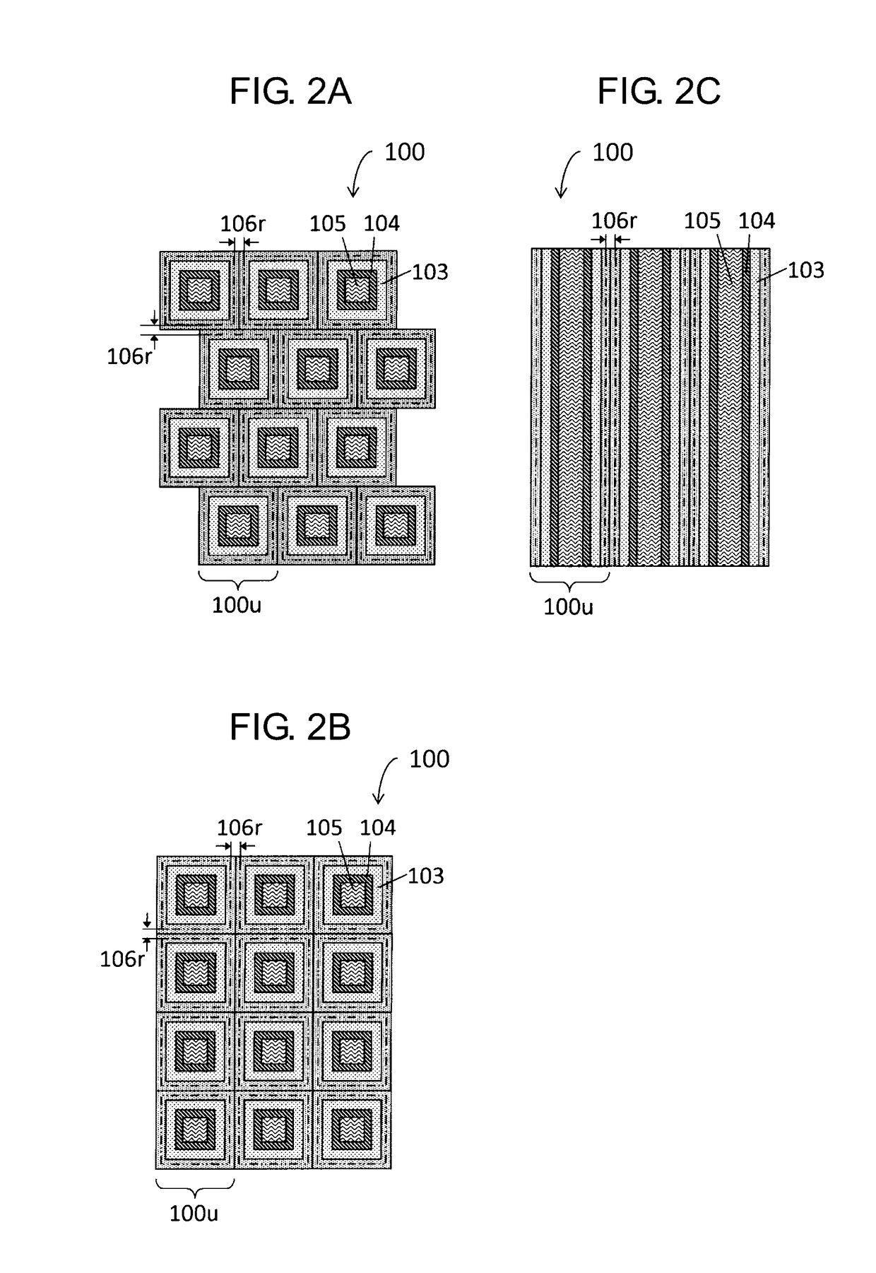
[0113]FIG. 8A schematically illustrates a cross-section of silicon carbide semiconductor element 200 according to the second exemplary embodiment. Silicon carbide semiconductor element 200 includes a plurality of unit cells 200u. In the present second exemplary embodiment, channel removed region 106r is set to be deeper than the first exemplary embodiment. Specifically, while channel removed region 106r in the first exemplary embodiment is a cutout of second silicon carbide semiconductor layer 106, channel removed region 106r in the present second exemplary embodiment includes not only the cutout of second silicon carbide semiconductor layer 106 but also a cutout of JFET region 102j. The cutout of JFET region 102j is extended from the upper surface of JFET region 102j, and is spatially continuous with the cutout of second silicon carbide semiconductor layer 106. Note that the processes other than the channel removing process are similar to those in the first exemplary embodiment. As...


PUM


Abstract

In the silicon carbide semiconductor element, a second silicon carbide semiconductor layer that is in contact with the surface of a first silicon carbide semiconductor layer has at least an upper layer including a dopant of a first conductivity type at a high concentration. Above a junction field effect transistor (JFET) region interposed between body regions that are disposed in the first silicon carbide semiconductor layer so as to be spaced from each other, the silicon carbide semiconductor element has a channel removed region, which is a cutout formed by removing a high concentration layer from the front surface side of the second silicon carbide semiconductor layer, the high concentration layer having a higher dopant concentration than at least the dopant concentration of the JFET region. The width of the channel removed region is smaller than that of the JFET region.

Description

BACKGROUND[0001]1. Technical Field[0002]The present disclosure relates to a semiconductor element, and more particularly to a silicon carbide semiconductor element such as a power semiconductor device used for high breakdown voltage and large current, and a method for manufacturing the silicon carbide semiconductor element.[0003]2. Description of the Related Art[0004]Silicon carbide (SiC) is a high-hardness semiconductor material having a band gap larger than that of silicon (Si), and is applied to various semiconductor devices such as a power element, an environmentally-resistant element, a high-temperature operation element, and a high-frequency element. Among these elements, application to power elements, such as a semiconductor element and a rectifier element, is gaining attention. Power elements using SiC have an advantage that they can significantly reduce power loss, compared to power elements using Si. In addition, by utilizing such properties, SiC power elements can impleme...

Claims


Application Information

Patent Timeline
IPC IPC(8): H01L29/78H01L29/66H01L29/10H01L29/16H01L27/06
CPCH01L29/7803H01L29/1608H01L27/0617H01L29/80H01L29/105H01L29/66068H01L29/1095H01L29/42368H01L29/7828H01L29/0696H01L29/0878
Inventor OHOKA, ATSUSHIUCHIDA, MASAOHORIKAWA, NOBUYUKIKUSUMOTO, OSAMU
Owner PANASONIC INTELLECTUAL PROPERTY MANAGEMENT CO LTD
Why Eureka
Try Eureka