CMOS image sensor and fabrication method thereof

a stacked, image sensor technology, applied in the direction of diodes, semiconductor/solid-state device details, radiation controlled devices, etc., can solve the problems of large noise generation, small fill factor of existing cmos image sensors,

Active Publication Date: 2017-06-15
SEMICON MFG INT (SHANGHAI) CORP +1
View PDF5 Cites 17 Cited by
  • Summary
  • Abstract
  • Description
  • Claims
  • Application Information

AI Technical Summary

Benefits of technology

[0030]In one embodiment, when the number of sub-trenches in each etched trench 104 is greater than one, neighboring sub-trenches in each etched trench may be separated from each other and the bottoms of the sub-trenches may expose different portions of the surface of a same first electrode 102. Further, when each etched trench includes multiple sub-trenches, a capacitor may be formed in each sub-trench. In addition, the multiple capacitors formed in the sub-trenches of an etched trench may be electrically connected to a corresponding first electrode 102 and a corresponding second electrode formed subsequently. As such, the capacitance value between the two connection points, i.e. the first electrode 102 and the subsequently-formed second electrode, may be further improved. Moreover, an increase in the capacitance value may be helpful for reducing thermal noise generated during the operation of the CMOS image sensor. For example, an increase in the capacitance value may help to reduce kTC noise, which is known as a fluctuation noise of a resistor in a charging circuit due to temperature fluctuation during charging-and-discharging process.
[0030]In one embodiment, when the number of sub-trenches in each etched trench 104 is greater than one, neighboring sub-trenches in each etched trench may be separated from each other and the bottoms of the sub-trenches may expose different portions of the surface of a same first electrode 102. Further, when each etched trench includes multiple sub-trenches, a capacitor may be formed in each sub-trench. In addition, the multiple capacitors formed in the sub-trenches of an etched trench may be electrically connected to a corresponding first electrode 102 and a corresponding second electrode formed subsequently. As such, the capacitance value between the two connection points, i.e. the first electrode 102 and the subsequently-formed second electrode, may be further improved. Moreover, an increase in the capacitance value may be helpful for reducing thermal noise generated during the operation of the CMOS image sensor. For example, an increase in the capacitance value may help to reduce kTC noise, which is known as a fluctuation noise of a resistor in a charging circuit due to temperature fluctuation during charging-and-discharging process.
[0030]In one embodiment, when the number of sub-trenches in each etched trench 104 is greater than one, neighboring sub-trenches in each etched trench may be separated from each other and the bottoms of the sub-trenches may expose different portions of the surface of a same first electrode 102. Further, when each etched trench includes multiple sub-trenches, a capacitor may be formed in each sub-trench. In addition, the multiple capacitors formed in the sub-trenches of an etched trench may be electrically connected to a corresponding first electrode 102 and a corresponding second electrode formed subsequently. As such, the capacitance value between the two connection points, i.e. the first electrode 102 and the subsequently-formed second electrode, may be further improved. Moreover, an increase in the capacitance value may be helpful for reducing thermal noise generated during the operation of the CMOS image sensor. For example, an increase in the capacitance value may help to reduce kTC noise, which is known as a fluctuation noise of a resistor in a charging circuit due to temperature fluctuation during charging-and-discharging process.
[0030]In one embodiment, when the number of sub-trenches in each etched trench 104 is greater than one, neighboring sub-trenches in each etched trench may be separated from each other and the bottoms of the sub-trenches may expose different portions of the surface of a same first electrode 102. Further, when each etched trench includes multiple sub-trenches, a capacitor may be formed in each sub-trench. In addition, the multiple capacitors formed in the sub-trenches of an etched trench may be electrically connected to a corresponding first electrode 102 and a corresponding second electrode formed subsequently. As such, the capacitance value between the two connection points, i.e. the first electrode 102 and the subsequently-formed second electrode, may be further improved. Moreover, an increase in the capacitance value may be helpful for reducing thermal noise generated during the operation of the CMOS image sensor. For example, an increase in the capacitance value may help to reduce kTC noise, which is known as a fluctuation noise of a resistor in a charging circuit due to temperature fluctuation during charging-and-discharging process.

Problems solved by technology

Specifically, the fill factor in existing CMOS image sensors may be relatively small and noise (such as kTC thermal noise) may be generated during the operation of the CMOS image sensors.

Method used


Image

  • CMOS image sensor and fabrication method thereof
  • CMOS image sensor and fabrication method thereof
  • CMOS image sensor and fabrication method thereof

Examples


Embodiment Construction

[0014]Reference will now be made in detail to exemplary embodiments of the invention, which are illustrated in the accompanying drawings. Wherever possible, the same reference numbers will be used throughout the drawings to refer to the same or like parts.

[0015]FIG. 16 shows a flowchart of an exemplary fabrication process for an exemplary CMOS image sensor consistent with disclosed embodiments. FIGS. 1-14 show schematic views of semiconductor structures corresponding to certain stages of the exemplary fabrication method.

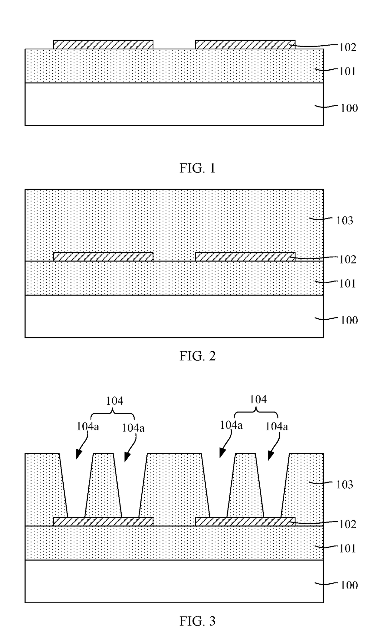
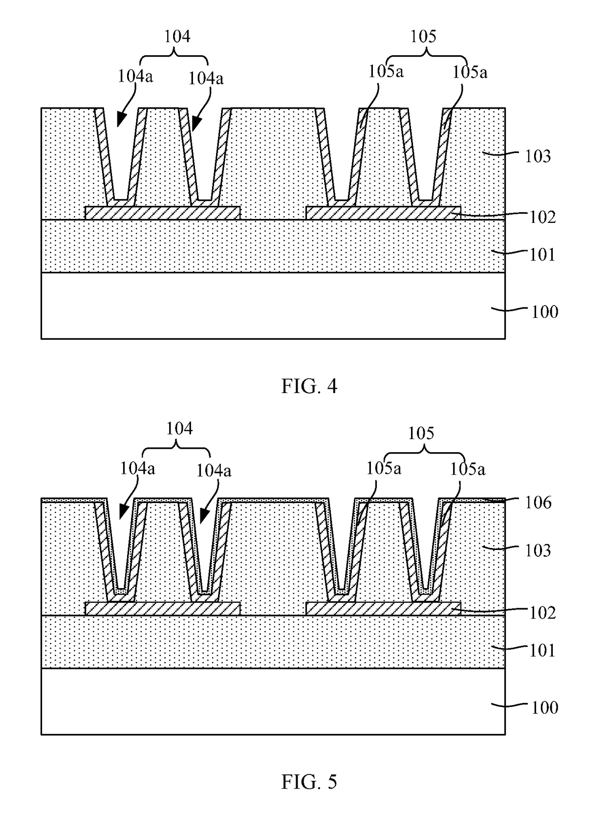
[0016]In FIG. 16, at the beginning of the fabrication process, a first substrate is provided (S101). FIG. 1 shows a schematic view of a corresponding semiconductor substrate.

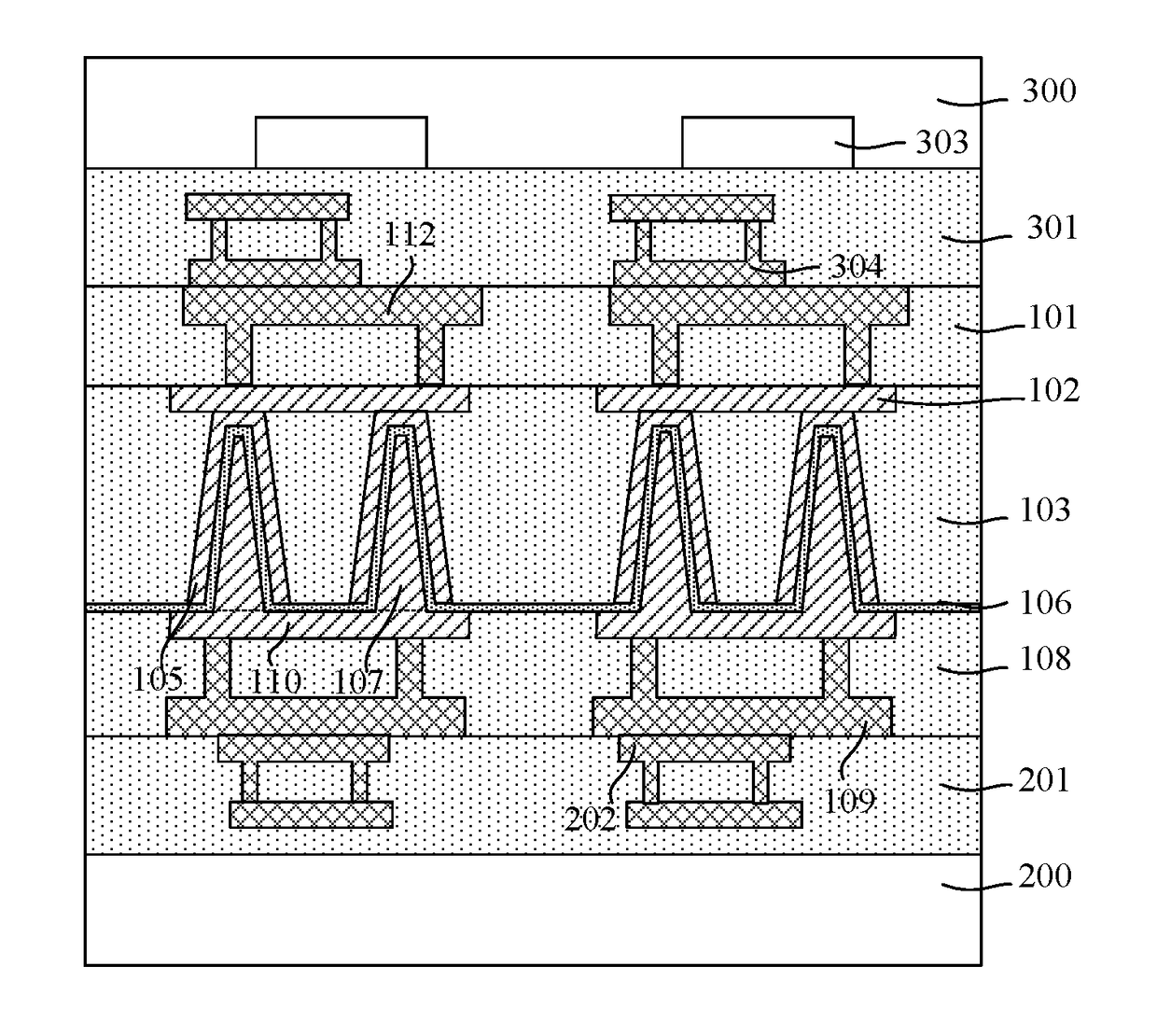
[0017]Referring to FIG. 1, a first substrate 100 is provided. A first dielectric layer 101 may be formed on the first substrate 100. A plurality of discrete first electrodes 102 may be formed on the first dielectric layer 101.

[0018]The first substrate 100 may be used as a carrier substrate for su...


PUM


Abstract

A method to form a stacked CMOS image sensor includes forming a signal processing layer including a plurality of discrete signal processing circuit, an image sensor layer including a plurality of discrete image sensing units, and an intermediate capacitor layer including a dielectric layer and a plurality of capacitors. Each capacitor includes a first electrode, a V-shaped or U-shaped first electrode material layer electrically connecting to the first electrode, a second electrode material layer on the first electrode material layer having the dielectric layer there-between, and a second electrode electrically connecting to the second electrode material layer. The method further includes bonding the signal processing layer to the intermediate capacitor layer with each second electrode electrically connected to a signal processing circuit, and bonding the image sensor layer to the intermediate capacitor layer with each first electrode electrically connected to an image sensing unit.

Description

CROSS-REFERENCES TO RELATED APPLICATIONS[0001]This application claims the priority of Chinese Patent Application No. CN201510916698.6, filed on Dec. 10, 2015, the entire content of which is incorporated herein by reference.FIELD OF THE DISCLOSURE[0002]The present disclosure generally relates to the field of image sensing technology and, more particularly, relates to a stacked CMOS image sensor and fabrication methods thereof.BACKGROUND[0003]With fast development of electrical and electronical technology, more and more modern mobile electronic products that use image sensor technology, such as smart phones, digital cameras, notebook computers, etc., have been rapidly developed and widely used. Currently, people spend significantly increased time on mobile phones and other electronic products and, tend to have more and more demands on product quality and personal experience. Today, most electronic devices are capable for snapping pictures and taking videos, and the total number of pix...

Claims


Application Information

Patent Timeline
Patent Type & Authority Applications(United States)
IPC IPC(8): H01L27/146H01L23/522
CPCH01L27/14636H01L23/5223H01L28/90H01L27/14634H01L27/1464H01L27/1469H01L21/28H01L21/768H01L23/522H01L27/146H01L27/14643H01L27/14683H01L27/14689H01L27/0688H01L27/14609H01L28/91H01L21/8221H01L23/642
Inventor HUANG, HERB HEDROWLEY, CLIFFORD IANGAO, GUAN QIEBAO, DE JUN
Owner SEMICON MFG INT (SHANGHAI) CORP
Why Eureka
Try Eureka