Patterns of fluorescent seeded nanorods

a technology of seeded nanorods and patterns, which is applied in the direction of crystal growth process, polycrystalline material growth, instruments, etc., can solve the problem of limit the use of qds in printing applications, and achieve high performance operation, good adhesion to the substrate, and high optical and chemical stability

Inactive Publication Date: 2017-06-22
YISSUM RES DEV CO OF THE HEBREWUNIVERSITY OF JERUSALEM LTD
View PDF2 Cites 1 Cited by
  • Summary
  • Abstract
  • Description
  • Claims
  • Application Information

AI Technical Summary

Benefits of technology

[0036]4. Reduced self-absorption: The pattern has substantially reduced or diminished undesired absorption of light emitted by the pattern itself (re-absorption).
[0121]As indicated herein, the patterned films according to the invention exhibit higher optical and chemical stability and thus may be used in a variety of applications. Such applications may in particular include fluorescent signage, optoelectronic applications and devices. Due to the special advantages of the patterned films, devices based on such films exhibit high performance operation.

Problems solved by technology

The inventors of the technology disclosed herein have found that the effects associated with quantum dots (QDs), and which have been summarized in the background, present a limitation for the use of QDs in printing applications, in which maintaining high efficiency of fluorescence along with the control of optical properties is crucial.

Method used


Image

  • Patterns of fluorescent seeded nanorods
  • Patterns of fluorescent seeded nanorods
  • Patterns of fluorescent seeded nanorods

Examples


Embodiment Construction

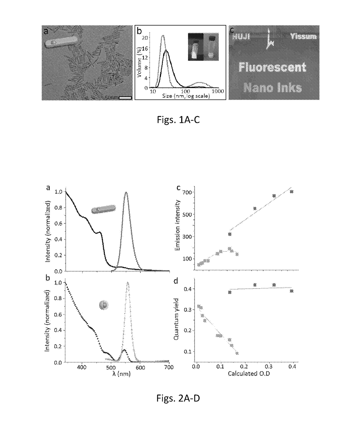
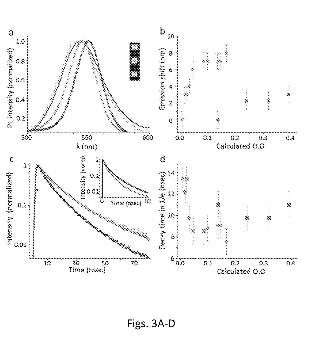
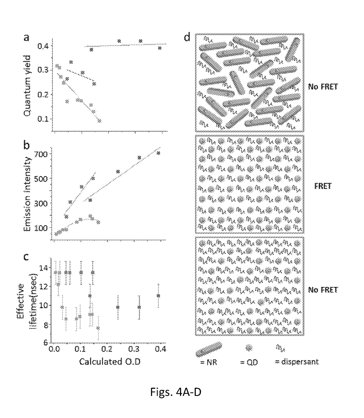
[0152]Semiconductor nanocrystals exhibit unique fluorescent properties which are tunable by size, shape and composition. The high quantum yield and enhanced stability led to their use in biomedical imaging and flat panel displays. Here, semiconductor nanorods based inkjet inks are presented, overcoming limitations of the commonly reported quantum dots in printing applications. Fluorescent seeded nanorods were found to be outstanding candidates for fluorescent inks, due to their low particle-particle interactions and negligible self-absorption. This is manifested by insignificant emission shifts upon printing, even at highly concentrated printed layers and by maintaining the high fluorescence quantum yield, unlike quantum dots which exhibit fluorescent wavelengths shifts and quenching effects. This behavior results from the reduced absorption / emission overlap, accompanied by low energy transfer efficiencies between the nanorods as supported by steady state and time resolved fluoresce...


PUM

PropertyMeasurementUnit
sizeaaaaaaaaaa
sizeaaaaaaaaaa
sizeaaaaaaaaaa

Abstract

Provided are printed patterns and objects including, for example, a film or 3D object, which may include one or more nanorods. According to the subject matter provided, the nanorods may reduce or diminish inter-particle interaction in the pattern or object.

Description

TECHNOLOGICAL FIELD[0001]The invention generally relates to processes for constructing patterns of seeded nanorods.BACKGROUND ART[0002]In the last few years, fluorescent semiconductor nanocrystals (NCs) have developed greatly in terms of control of their size, shape and composition, providing exceptional control over their properties, allowing for their implementation in a variety of applications such as displays.[0003]The NCs are characterized by a wide absorption spectrum accompanied by a narrow and sharp emission spectrum at the band edge, which enable the simultaneous excitation of NCs with different emission wavelengths using the same lighting source. The fluorescent semiconductor NCs also show outstanding optical and chemical stability under light irradiation over long periods of time. In addition, they are easily adapted to specific applications by the ability to design and control the emission color and properties by tuning their size, shape and composition. Their surface ch...

Claims


Application Information

Patent Timeline
Patent Type & Authority Applications(United States)
IPC IPC(8): C30B29/50C09D11/50C30B7/14C09D11/037B41J2/045C30B29/62C09K11/88C09D11/322
CPCC30B29/50Y10S977/95C09D11/50C09D11/322C09D11/037B41J2/04581C30B29/62C30B7/14B82Y40/00B82Y30/00Y10S977/762Y10S977/774Y10S977/824Y10S977/892C09K11/883B82B1/00B82B3/0004B82B3/0038G02B1/02
Inventor BANIN, URIMAGDASSI, SHLOMOSHEMESH, SHAIHALIVNI, SHIRAVINETSKY, YELENA
Owner YISSUM RES DEV CO OF THE HEBREWUNIVERSITY OF JERUSALEM LTD
Why Eureka
Try Eureka