

Multi-type BGA Chip Visual Recognition Method Using Line Based Clustering
a multi-type, chip technology, applied in image enhancement, image analysis, instruments, etc., can solve the problems of chip defects, oversize or undersize balls, extra balls, etc., to achieve strong flexibility, improve the robustness of the algorithm to background interference, and ensure the accuracy of recognition results.
- Summary
- Abstract
- Description
- Claims
- Application Information
AI Technical Summary
Benefits of technology
Problems solved by technology
Method used
Image

Examples
embodiment 1
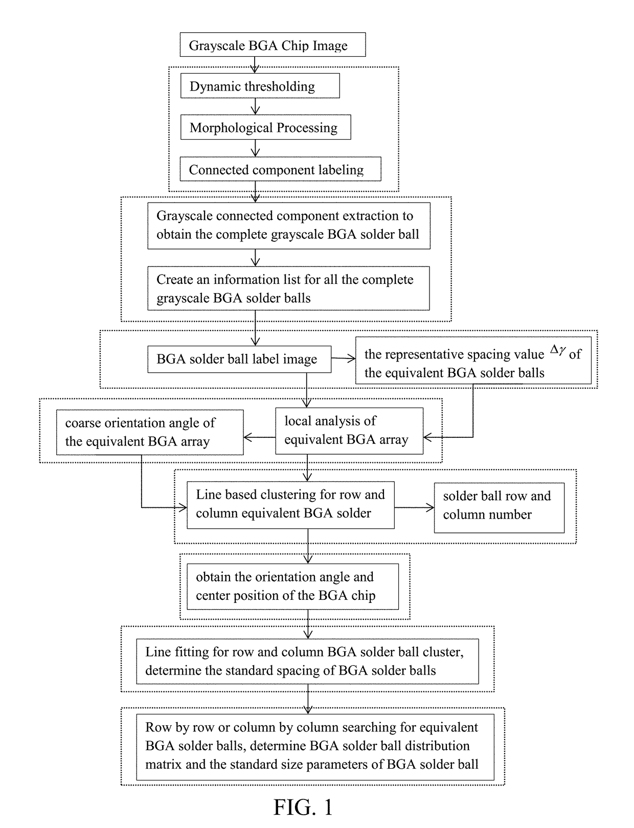
[0044]According to this preferred embodiment 1, a multi-type BGA chip visual recognition using line based clustering comprises the following steps:
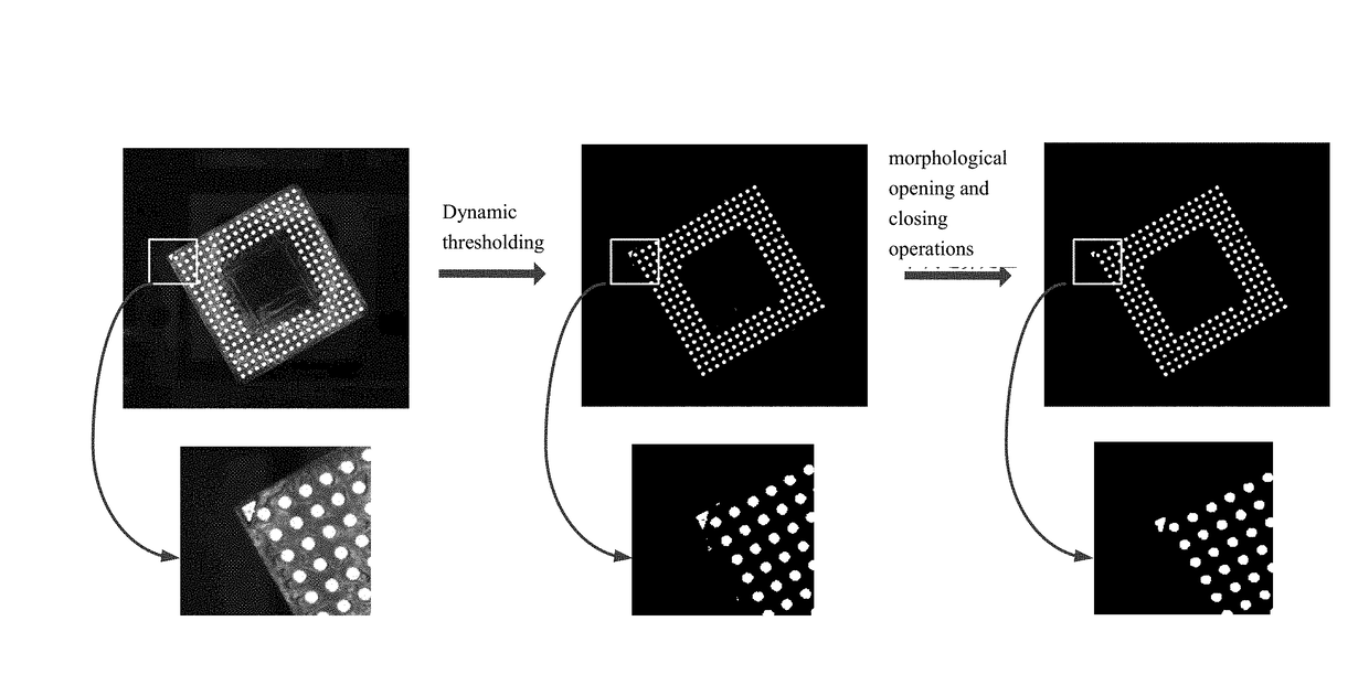
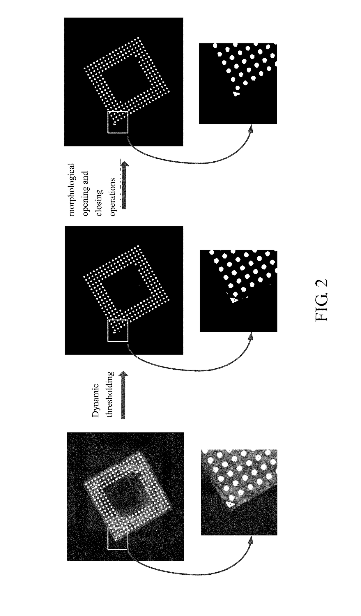
[0045]Step 1: defining a grayscale BGA chip image acquired from a camera as an original image, performing dynamic thresholding to obtain binary image of solder balls, performing morphological opening and closing operations to the binary image of solder balls, defining each connected component on the processed binary image of solder balls as a binary BGA solder ball, then performing connected component labeling for each binary BGA solder ball;
[0046]Wherein a mathematical express of processing the original image through dynamic thresholding to obtain the binary image of solder balls I(x, y) is as follows:
I(x,y)={1f(x,y)≥g(x,y)+C0f(x,y)<g(x,y)+C
[0047]In the above formula, f (x, y) refers to the original image, g(x, y) refers to the image after applying mean filtering to f (x, y). C refers to the preset constant.
[0048]Step 2: for each bina...
embodiment 2
[0058]The difference between this embodiment and embodiment 1 is that: in the step 2, the information list for all complete grayscale BGA solder balls includes the following specific data:
[0059](1) grayscale pixels of each complete grayscale BGA solder ball: the process of grayscale connected component extraction on a corresponding area in the original image is based on the following formula:
(xp,yp){∈Rf(xp,yp)-mean[R]<ϛ&&∃(xadj,yadj)∈R,f(xp,yp)-f(xadj,yadj)<Δ∉Relse
[0060]In the above formula, (xp, yp) refers respectively to the horizontal and vertical coordinates defined on the original image, R refers to the pixel set of current grayscale BGA solder ball, mean[R] refers to the mean grayscale value of all pixels in the current grayscale BGA solder ball, (xadj, yadj) refers to the coordinates which is adjacent in 8-conectivity to (xp, yp) which is already belonged to the pixels of R, ζ and Δ refers to the preset constant; f (xp, yp) refers to the grayscale value at the p...
embodiment 3
[0066]the difference between this embodiment and embodiment 1 or 2 is that: in the step 4, the specific process for local analysis of regular type BGA chips is typically illustrated in FIG. 3(a):
[0067]Step 4-1: in the BGA solder ball label image, select any equivalent BGA solder ball;
[0068]Step 4-2: define the equivalent BGA solder ball selected in the step 4-1 as a center, within the radius range of 3Δγ, search within the scope of four directions of)) [−45°, 45°), [45°, 135°), [135°, 225°) and [−135°, −45°) respectively to locate the closest equivalent BGA solder ball to the equivalent BGA solder ball selected in the step 4-1, if the closest equivalent BGA solder ball in the four directions does not exist, repeat the step 4-1;
[0069]Step 4-3: for the closest adjacent equivalent BGA solder ball at each direction, the coarse orientation angle Δθ of equivalent BGA array corresponding to the j direction is obtained by the following formula:
Δθj=±arctan(yadjj-ycenterxadjj-xcenter)±90∘
[007...
PUM
 Abstract
Description
Claims
Application Information